
Users Manual
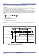
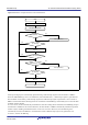
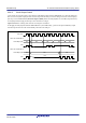
Table Of Contents
- 34. IrDA Interface
- 35. I2C-bus Interface (RIICa)
- 35.1 Overview
- 35.2 Register Descriptions
- 35.2.1 I2C-bus Control Register 1 (ICCR1)
- 35.2.2 I2C-bus Control Register 2 (ICCR2)
- 35.2.3 I2C-bus Mode Register 1 (ICMR1)
- 35.2.4 I2C-bus Mode Register 2 (ICMR2)
- 35.2.5 I2C-bus Mode Register 3 (ICMR3)
- 35.2.6 I2C-bus Function Enable Register (ICFER)
- 35.2.7 I2C-bus Status Enable Register (ICSER)
- 35.2.8 I2C-bus Interrupt Enable Register (ICIER)
- 35.2.9 I2C-bus Status Register 1 (ICSR1)
- 35.2.10 I2C-bus Status Register 2 (ICSR2)
- 35.2.11 Slave Address Register Ly (SARLy) (y = 0 to 2)
- 35.2.12 Slave Address Register Uy (SARUy) (y = 0 to 2)
- 35.2.13 I2C-bus Bit Rate Low-Level Register (ICBRL)
- 35.2.14 I2C-bus Bit Rate High-Level Register (ICBRH)
- 35.2.15 I2C-bus Transmit Data Register (ICDRT)
- 35.2.16 I2C-bus Receive Data Register (ICDRR)
- 35.2.17 I2C-bus Shift Register (ICDRS)
- 35.3 Operation
- 35.4 SCL Synchronization Circuit
- 35.5 SDA Output Delay Function
- 35.6 Digital Noise Filters
- 35.7 Address Match Detection
- 35.8 Automatic Low-Hold Function for SCL
- 35.9 Arbitration-Lost Detection Functions
- 35.10 Start Condition/Restart Condition/Stop Condition Generating Function
- 35.11 Bus Hanging
- 35.12 SMBus Operation
- 35.13 Interrupt Sources
- 35.14 Initialization of Registers and Functions When a Reset is Applied or a Condition is Detected
- 35.15 Event Link Function (Output)
- 35.16 Usage Notes
- 36. CAN Module (RSCAN)

R01UH0823EJ0110 Rev.1.10 Page 1060 of 1852
Nov 30, 2020
RX23W Group 33. Serial Communications Interface (SCIg, SCIh)
33.6.4 Receive Data Sampling Timing and Reception Margin
Only the base clock generated by the on-chip baud rate generator can be used as a transmit/receive clock in smart card
interface mode.
In this mode, the SCI can operate on a base clock with a frequency of 32, 64, 372, 256, 93, 128, 186, or 512 times the bit
rate according to the settings of the SCMR.BCP2 bit and the SMR.BCP[1:0] bits.
For data reception, the falling edge of the start bit is sampled with the base clock to perform synchronization. Receive
data is sampled on the 16th, 32nd, 186th, 128th, 46th, 64th, 93rd, and 256th rising edges of the base clock so that it can
be latched at the middle of each bit as shown in
Figure 33.37. The reception margin here is determined by the following
formula.
(%)
M: Reception margin (%)
N: Ratio of bit rate to clock (N = 32, 64, 372, 256)
D: Duty cycle of clock (D = 0 to 1.0)
L: Frame length (L = 10)
F: Absolute value of clock frequency deviation
Assuming values of F = 0, D = 0.5, and N = 372 in the above formula, the reception margin is determined by the formula
below.
M = {0.5 – 1/(2 × 372)} × 100 (%) = 49.866 (%)
Figure 33.37 Receive Data Sampling Timing in Smart Card Interface Mode
(When Clock Frequency is 372 Times the Bit Rate)
M0.5
1
2N
--------–
L0.5–()F–
D0.5–
N
---------------------
1F+()– 100×=
Base clock
372 clocks
186 clocks
D0 D1
185 371 0371185 00
Receive data (RXDn)
Synchronization sampling
timing
Data sampling timing
Start bit
186 clocks
372 clocks