
Users Manual
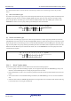
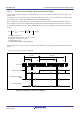
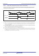
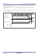
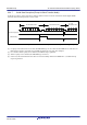
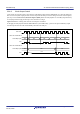
Table Of Contents
- 34. IrDA Interface
- 35. I2C-bus Interface (RIICa)
- 35.1 Overview
- 35.2 Register Descriptions
- 35.2.1 I2C-bus Control Register 1 (ICCR1)
- 35.2.2 I2C-bus Control Register 2 (ICCR2)
- 35.2.3 I2C-bus Mode Register 1 (ICMR1)
- 35.2.4 I2C-bus Mode Register 2 (ICMR2)
- 35.2.5 I2C-bus Mode Register 3 (ICMR3)
- 35.2.6 I2C-bus Function Enable Register (ICFER)
- 35.2.7 I2C-bus Status Enable Register (ICSER)
- 35.2.8 I2C-bus Interrupt Enable Register (ICIER)
- 35.2.9 I2C-bus Status Register 1 (ICSR1)
- 35.2.10 I2C-bus Status Register 2 (ICSR2)
- 35.2.11 Slave Address Register Ly (SARLy) (y = 0 to 2)
- 35.2.12 Slave Address Register Uy (SARUy) (y = 0 to 2)
- 35.2.13 I2C-bus Bit Rate Low-Level Register (ICBRL)
- 35.2.14 I2C-bus Bit Rate High-Level Register (ICBRH)
- 35.2.15 I2C-bus Transmit Data Register (ICDRT)
- 35.2.16 I2C-bus Receive Data Register (ICDRR)
- 35.2.17 I2C-bus Shift Register (ICDRS)
- 35.3 Operation
- 35.4 SCL Synchronization Circuit
- 35.5 SDA Output Delay Function
- 35.6 Digital Noise Filters
- 35.7 Address Match Detection
- 35.8 Automatic Low-Hold Function for SCL
- 35.9 Arbitration-Lost Detection Functions
- 35.10 Start Condition/Restart Condition/Stop Condition Generating Function
- 35.11 Bus Hanging
- 35.12 SMBus Operation
- 35.13 Interrupt Sources
- 35.14 Initialization of Registers and Functions When a Reset is Applied or a Condition is Detected
- 35.15 Event Link Function (Output)
- 35.16 Usage Notes
- 36. CAN Module (RSCAN)

R01UH0823EJ0110 Rev.1.10 Page 1059 of 1852
Nov 30, 2020
RX23W Group 33. Serial Communications Interface (SCIg, SCIh)
For communications with IC cards of the direct convention type and inverse convention type, follow the procedure
below.
(1) Direct Convention Type
For the direct convention type, logic levels 1 and 0 correspond to states Z and A, respectively, and data is transferred with
LSB first as the start character, as shown in
Figure 33.35. Therefore, data in the start character in the figure is 3Bh.
When using the direct convention type, write 0 to both the SDIR and SINV bits in the SCMR register. Write 0 to the
SMR.PM bit in order to use even parity, which is prescribed by the smart card standard.
Figure 33.35 Direct Convention (SCMR.SDIR bit = 0, SCMR.SINV bit = 0, SMR.PM bit = 0)
(2) Inverse Convention Type
For the inverse convention type, logic levels 1 and 0 correspond to states A and Z, respectively and data is transferred
with MSB first as the start character, as shown in
Figure 33.36. Therefore, data in the start character in the figure is 3Fh.
When using the inverse convention type, write 1 to both the SDIR and SINV bits in the SCMR register. The parity bit is
logic level 0 to produce even parity, which is prescribed by the smart card standard, and corresponds to state Z. Since the
SINV bit of the this MCU only inverts data bits D7 to D0, write 1 to the SMR.PM bit to invert the parity bit for both
transmission and reception.
Figure 33.36 Inverse Convention (SCMR.SDIR bit = 1, SCMR.SINV bit = 1, SMR.PM bit = 1)
33.6.3 Block Transfer Mode
Block transfer mode is different from non-block transfer mode in the following respects.
• Even if a parity error is detected during reception, no error signal is output. Since the SSR.PER flag is set by error
detection, clear the PER flag before receiving the parity bit of the next frame.
• During transmission, at least 1 etu is secured as a guard time from the end of the parity bit until the start of the next
frame.
• Since the same data is not retransmitted during transmission, the SSR.TEND flag is set 11.5 etu after transmission
start.
• In block transfer mode, the SSR.ERS flag indicates the error signal status as in non-block transfer mode, but the flag
is read as 0 because no error signal is transferred.
Ds
AZZAZZ ZZAA
(Z)
(Z) state
D0 D1 D2 D3 D4 D5 D6 D7 Dp
Ds
AZZAAA ZAAA
D7 D6 D5 D4 D3 D2 D1 D0 Dp
(Z) (Z) state