
Users Manual
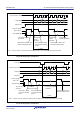
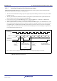
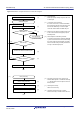
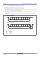
Table Of Contents
- 34. IrDA Interface
- 35. I2C-bus Interface (RIICa)
- 35.1 Overview
- 35.2 Register Descriptions
- 35.2.1 I2C-bus Control Register 1 (ICCR1)
- 35.2.2 I2C-bus Control Register 2 (ICCR2)
- 35.2.3 I2C-bus Mode Register 1 (ICMR1)
- 35.2.4 I2C-bus Mode Register 2 (ICMR2)
- 35.2.5 I2C-bus Mode Register 3 (ICMR3)
- 35.2.6 I2C-bus Function Enable Register (ICFER)
- 35.2.7 I2C-bus Status Enable Register (ICSER)
- 35.2.8 I2C-bus Interrupt Enable Register (ICIER)
- 35.2.9 I2C-bus Status Register 1 (ICSR1)
- 35.2.10 I2C-bus Status Register 2 (ICSR2)
- 35.2.11 Slave Address Register Ly (SARLy) (y = 0 to 2)
- 35.2.12 Slave Address Register Uy (SARUy) (y = 0 to 2)
- 35.2.13 I2C-bus Bit Rate Low-Level Register (ICBRL)
- 35.2.14 I2C-bus Bit Rate High-Level Register (ICBRH)
- 35.2.15 I2C-bus Transmit Data Register (ICDRT)
- 35.2.16 I2C-bus Receive Data Register (ICDRR)
- 35.2.17 I2C-bus Shift Register (ICDRS)
- 35.3 Operation
- 35.4 SCL Synchronization Circuit
- 35.5 SDA Output Delay Function
- 35.6 Digital Noise Filters
- 35.7 Address Match Detection
- 35.8 Automatic Low-Hold Function for SCL
- 35.9 Arbitration-Lost Detection Functions
- 35.10 Start Condition/Restart Condition/Stop Condition Generating Function
- 35.11 Bus Hanging
- 35.12 SMBus Operation
- 35.13 Interrupt Sources
- 35.14 Initialization of Registers and Functions When a Reset is Applied or a Condition is Detected
- 35.15 Event Link Function (Output)
- 35.16 Usage Notes
- 36. CAN Module (RSCAN)

R01UH0823EJ0110 Rev.1.10 Page 1056 of 1852
Nov 30, 2020
RX23W Group 33. Serial Communications Interface (SCIg, SCIh)
33.5.6 Simultaneous Serial Data Transmission and Reception (Clock Synchronous
Mode)
Figure 33.32 shows a sample flowchart for simultaneous serial transmit and receive operations in clock synchronous
mode.
After initializing the SCI, the following procedure should be used for simultaneous serial data transmit and receive
operations.
To switch from transmit mode to simultaneous transmit and receive mode, check that the SCI has finished transmission
by reading that the SSR.TEND flag is 1, and then initialize the SCR register. Then set the TIE, RIE, TE, and RE bits in
the SCR register to 1 simultaneously by a single instruction.
To switch from receive mode to simultaneous transmit and receive mode, check that the SCI has finished reception, and
then set the RIE and RE bits to 0. Then check that the receive error flags (ORER, FER, and PER in the SSR register) are
0, and then set the TIE, RIE, TE, and RE bits in the SCR register to 1 simultaneously by a single instruction.
Figure 33.32 Example Flowchart of Simultaneous Serial Transmission and Reception in Clock Synchronous
Mode
Yes
End
No
Initialization
Start data transmission/reception
Error processing
Read receive data in the RDR
register
No
Yes
SSR.ORER = 1
All data received?
No
Yes
TXI interrupt
Write transmit data to the TDR
register
No
Yes
RXI interrupt
Read the SSR.ORER flag
Set the SCR.TIE, RIE, TE, RE, and
TEIE bits to 0
[ 1 ]
[ 2 ]
[ 3 ]
[ 4 ]
[ 5 ]
[ 1 ] SCI initialization:
The TXDn pin can act as the output pin for
transmitted data and the RXDn pin can act as the
input pin for received data at the same time.
[ 2 ] Transmit data write:
Write transmit data to the TDR register once in
the TXI interrupt handling routine.
[ 3 ] Receive error processing:
If a receive error occurs, read the SSR.ORER
flag, perform the relevant error processing, and
then set the ORER flag to 0. Data reception
cannot be resumed while the ORER flag is 1.
[ 4 ] Reading receive data:
Read the receive data in the RDR register once in
the RXI interrupt request handling routine.
[ 5 ] Serial transmission/reception continuation
procedure:
To continue serial transmission and reception,
before the MSB (bit 7) of the current frame is
received, finish reading the receive data in the
RDR register by the RXI interrupt. Also, before
the MSB (bit 7) of the current frame is transmitted,
write data to the TDR register by the TXI interrupt.
Transmit data can also be written to the TDR
register by activating the DMAC or DTC by a
transmit data empty interrupt (TXI) request.
Similarly, the RDR data can also be read by
activating the DMAC or DTC by a receive data full
interrupt (RXI) request.
Note: When switching from transmit or receive operation to simultaneous transmit and receive operations first set the
TIE, RIE, TE, RE, and TEIE bits in the SCR register to 0, and then set TIE, RIE, TE, and RE bits to 1
simultaneously.