
Users Manual
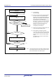
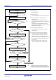
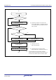
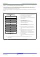
Table Of Contents
- 34. IrDA Interface
- 35. I2C-bus Interface (RIICa)
- 35.1 Overview
- 35.2 Register Descriptions
- 35.2.1 I2C-bus Control Register 1 (ICCR1)
- 35.2.2 I2C-bus Control Register 2 (ICCR2)
- 35.2.3 I2C-bus Mode Register 1 (ICMR1)
- 35.2.4 I2C-bus Mode Register 2 (ICMR2)
- 35.2.5 I2C-bus Mode Register 3 (ICMR3)
- 35.2.6 I2C-bus Function Enable Register (ICFER)
- 35.2.7 I2C-bus Status Enable Register (ICSER)
- 35.2.8 I2C-bus Interrupt Enable Register (ICIER)
- 35.2.9 I2C-bus Status Register 1 (ICSR1)
- 35.2.10 I2C-bus Status Register 2 (ICSR2)
- 35.2.11 Slave Address Register Ly (SARLy) (y = 0 to 2)
- 35.2.12 Slave Address Register Uy (SARUy) (y = 0 to 2)
- 35.2.13 I2C-bus Bit Rate Low-Level Register (ICBRL)
- 35.2.14 I2C-bus Bit Rate High-Level Register (ICBRH)
- 35.2.15 I2C-bus Transmit Data Register (ICDRT)
- 35.2.16 I2C-bus Receive Data Register (ICDRR)
- 35.2.17 I2C-bus Shift Register (ICDRS)
- 35.3 Operation
- 35.4 SCL Synchronization Circuit
- 35.5 SDA Output Delay Function
- 35.6 Digital Noise Filters
- 35.7 Address Match Detection
- 35.8 Automatic Low-Hold Function for SCL
- 35.9 Arbitration-Lost Detection Functions
- 35.10 Start Condition/Restart Condition/Stop Condition Generating Function
- 35.11 Bus Hanging
- 35.12 SMBus Operation
- 35.13 Interrupt Sources
- 35.14 Initialization of Registers and Functions When a Reset is Applied or a Condition is Detected
- 35.15 Event Link Function (Output)
- 35.16 Usage Notes
- 36. CAN Module (RSCAN)

R01UH0823EJ0110 Rev.1.10 Page 1048 of 1852
Nov 30, 2020
RX23W Group 33. Serial Communications Interface (SCIg, SCIh)
33.5.3 SCI Initialization (Clock Synchronous Mode)
Before transmitting and receiving data, start by writing the initial value 00h to the SCR register and then continue
through the procedure for SCI given in
Figure 33.24. Whenever the operating mode or transfer format is changed, the
SCR register must be initialized before the change is made.
Note that setting the SCR.RE bit to 0 initializes neither the ORER, FER, and PER flags in the SSR register nor the RDR
register.
Figure 33.24 Example of SCI Initialization Flowchart (Clock Synchronous Mode)
[ 1 ] Make I/O port settings to enable input and output functions
as required for TXDn, RXDn, and SCKn pins.
[ 2 ] Set the clock selection in the SCR register.
When an internal clock is selected, the SCK pin functions as
the clock output pin.
[ 3 ] Set the SIMR1.IICM bit to 0.
Set the SPMR.CKPH and CKPOL bits to 0.
Step [3] can be skipped if the values have not been
changed from the initial values.
[ 4 ] Set the data transmission/reception format in the SMR,
SCMR, and SEMR registers.
[ 5 ] Write a value corresponding to the bit rate to the BRR
register. This step is not necessary if an external clock is
used.
[ 6 ] Write the value obtained by correcting a bit rate error in the
MDDR register. This step is not necessary if the
SEMR.BRME bit is set to 0 or an external clock is used.
[ 7 ] Set the SCR.TE or RE bit to 1. At this time, also set the
SCR.TIE and RIE bits.
Setting the TE and RE bits allows TXDn and RXDn to be
used.
Start initialization
Set the SCR.TIE, RIE, TE, RE, and TEIE bits
to 0
Set the I/O port functions
Set the SCR.CKE[1:0] bits
[ 1 ]
[ 2 ]
Set the SIMR1.IICM bit to 0
Set the SPMR.CKPH and CKPOL bits to 0
[ 3 ]
Set data transmission/reception format in
the SMR, SCMR, and SEMR registers
[ 4 ]
Set a value in the BRR register
[ 5 ]
Set a value in the MDDR register
[ 6 ]
Set the SCR.TE or RE bit to 1, and
set the SCR.TIE and RIE bits
[ 7 ]
Transmission/reception
Note: In simultaneous transmit and receive operations, the SCR.TE and RE bits should both be set to 0 or 1
simultaneously.