
Users Manual
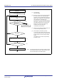
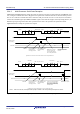
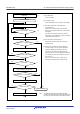
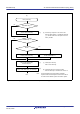
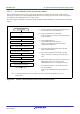
Table Of Contents
- 34. IrDA Interface
- 35. I2C-bus Interface (RIICa)
- 35.1 Overview
- 35.2 Register Descriptions
- 35.2.1 I2C-bus Control Register 1 (ICCR1)
- 35.2.2 I2C-bus Control Register 2 (ICCR2)
- 35.2.3 I2C-bus Mode Register 1 (ICMR1)
- 35.2.4 I2C-bus Mode Register 2 (ICMR2)
- 35.2.5 I2C-bus Mode Register 3 (ICMR3)
- 35.2.6 I2C-bus Function Enable Register (ICFER)
- 35.2.7 I2C-bus Status Enable Register (ICSER)
- 35.2.8 I2C-bus Interrupt Enable Register (ICIER)
- 35.2.9 I2C-bus Status Register 1 (ICSR1)
- 35.2.10 I2C-bus Status Register 2 (ICSR2)
- 35.2.11 Slave Address Register Ly (SARLy) (y = 0 to 2)
- 35.2.12 Slave Address Register Uy (SARUy) (y = 0 to 2)
- 35.2.13 I2C-bus Bit Rate Low-Level Register (ICBRL)
- 35.2.14 I2C-bus Bit Rate High-Level Register (ICBRH)
- 35.2.15 I2C-bus Transmit Data Register (ICDRT)
- 35.2.16 I2C-bus Receive Data Register (ICDRR)
- 35.2.17 I2C-bus Shift Register (ICDRS)
- 35.3 Operation
- 35.4 SCL Synchronization Circuit
- 35.5 SDA Output Delay Function
- 35.6 Digital Noise Filters
- 35.7 Address Match Detection
- 35.8 Automatic Low-Hold Function for SCL
- 35.9 Arbitration-Lost Detection Functions
- 35.10 Start Condition/Restart Condition/Stop Condition Generating Function
- 35.11 Bus Hanging
- 35.12 SMBus Operation
- 35.13 Interrupt Sources
- 35.14 Initialization of Registers and Functions When a Reset is Applied or a Condition is Detected
- 35.15 Event Link Function (Output)
- 35.16 Usage Notes
- 36. CAN Module (RSCAN)

R01UH0823EJ0110 Rev.1.10 Page 1045 of 1852
Nov 30, 2020
RX23W Group 33. Serial Communications Interface (SCIg, SCIh)
Figure 33.22 Example of Multi-Processor Serial Reception Flowchart (2)
End
Error processing
Yes
No
No
Yes
No
Yes
Framing error processing
Overrun error processing
SSR.ORER flag = 1
SSR.FER flag = 1
Break?
Set the SCR.RE bit to 0
[ 5 ]
Set the SSR.ORER, PER,
and FER flags to 0.
[ 7 ]
[ 7 ] Clearing the error flag:
Write 0 to the error flag.
[ 6 ]
[ 6 ] Processing in response to an overrun error:
Read the RDR register. In combination with step
[ 7 ], this will make correct reception of the next
frame possible.
Read the SSR.ORER, PER, and FER flags.
[ 8 ]
[ 8 ] Confirming that the error flag is cleared:
Read the error flag to confirm that its value is 0.
Note: The RDR register becomes the RDRH and RDRL
registers when 9-bit data length is selected. Read data in
the order from the RDRH register to the RDRL register.