
Users Manual
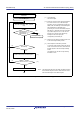
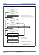
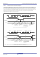
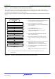
Table Of Contents
- 34. IrDA Interface
- 35. I2C-bus Interface (RIICa)
- 35.1 Overview
- 35.2 Register Descriptions
- 35.2.1 I2C-bus Control Register 1 (ICCR1)
- 35.2.2 I2C-bus Control Register 2 (ICCR2)
- 35.2.3 I2C-bus Mode Register 1 (ICMR1)
- 35.2.4 I2C-bus Mode Register 2 (ICMR2)
- 35.2.5 I2C-bus Mode Register 3 (ICMR3)
- 35.2.6 I2C-bus Function Enable Register (ICFER)
- 35.2.7 I2C-bus Status Enable Register (ICSER)
- 35.2.8 I2C-bus Interrupt Enable Register (ICIER)
- 35.2.9 I2C-bus Status Register 1 (ICSR1)
- 35.2.10 I2C-bus Status Register 2 (ICSR2)
- 35.2.11 Slave Address Register Ly (SARLy) (y = 0 to 2)
- 35.2.12 Slave Address Register Uy (SARUy) (y = 0 to 2)
- 35.2.13 I2C-bus Bit Rate Low-Level Register (ICBRL)
- 35.2.14 I2C-bus Bit Rate High-Level Register (ICBRH)
- 35.2.15 I2C-bus Transmit Data Register (ICDRT)
- 35.2.16 I2C-bus Receive Data Register (ICDRR)
- 35.2.17 I2C-bus Shift Register (ICDRS)
- 35.3 Operation
- 35.4 SCL Synchronization Circuit
- 35.5 SDA Output Delay Function
- 35.6 Digital Noise Filters
- 35.7 Address Match Detection
- 35.8 Automatic Low-Hold Function for SCL
- 35.9 Arbitration-Lost Detection Functions
- 35.10 Start Condition/Restart Condition/Stop Condition Generating Function
- 35.11 Bus Hanging
- 35.12 SMBus Operation
- 35.13 Interrupt Sources
- 35.14 Initialization of Registers and Functions When a Reset is Applied or a Condition is Detected
- 35.15 Event Link Function (Output)
- 35.16 Usage Notes
- 36. CAN Module (RSCAN)

R01UH0823EJ0110 Rev.1.10 Page 1044 of 1852
Nov 30, 2020
RX23W Group 33. Serial Communications Interface (SCIg, SCIh)
Figure 33.21 Example of Multi-Processor Serial Reception Flowchart (1)
Yes
End
No
Initialization
Start data reception
No
Yes
Set SCR.RE and RIE bits to 0
Error processing
(Continued to next page)
No
Yes
FER flag = 1 or ORER flag = 1
All data received?
Set SCR.MPIE bit to 1
Read the SSR.ORER and FER flags
Read receive data in the RDR register
No
Yes
Read SSR.ORER and FER flags
Yes
No
FER flag = 1 or ORER flag = 1
Yes
Read receive data in the RDR register
[ 1 ]
[ 2 ]
[ 3 ]
[ 4 ]
[ 5 ]
[ 1 ] SCI initialization:
Set data reception.
[ 2 ] ID reception cycle:
Set the SCR.MPIE bit to 1 and wait for ID reception.
[ 3 ] SCI status confirmation and reception and
comparison of ID:
Read data in the RDR register at the first RXI
interrupt, and compare it with the ID of the receiving
station itself.
If the ID does not match the ID of the receiving
station itself, set the MPIE bit to 1 again, and wait for
another RXI interrupt request.
[ 4 ] Data reception at an RXI interrupt:
Read data in the RDR register once in the RXI
interrupt routine.
[ 5 ] Receive error processing and break detection:
If a receive error occurs, an error is identified by
reading the ORER and FER flags in the SSR
register. After performing the appropriate error
processing, be sure to set the ORER and FER flags
to 0. Reception cannot be resumed if any of these
flags is set to 1.
In the case of a framing error, a break can be
detected by reading the value of the RXDn pin.
RXI interrupt?
No
ID of receiving station itself?
RXI interrupt?
Note: The RDR register becomes the RDRH and RDRL
registers when 9-bit data length is selected. Read data in
the order from the RDRH register to the RDRL register.