
Users Manual
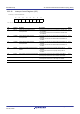
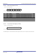
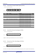
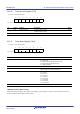
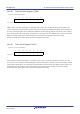
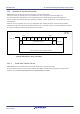
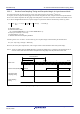
Table Of Contents
- 34. IrDA Interface
- 35. I2C-bus Interface (RIICa)
- 35.1 Overview
- 35.2 Register Descriptions
- 35.2.1 I2C-bus Control Register 1 (ICCR1)
- 35.2.2 I2C-bus Control Register 2 (ICCR2)
- 35.2.3 I2C-bus Mode Register 1 (ICMR1)
- 35.2.4 I2C-bus Mode Register 2 (ICMR2)
- 35.2.5 I2C-bus Mode Register 3 (ICMR3)
- 35.2.6 I2C-bus Function Enable Register (ICFER)
- 35.2.7 I2C-bus Status Enable Register (ICSER)
- 35.2.8 I2C-bus Interrupt Enable Register (ICIER)
- 35.2.9 I2C-bus Status Register 1 (ICSR1)
- 35.2.10 I2C-bus Status Register 2 (ICSR2)
- 35.2.11 Slave Address Register Ly (SARLy) (y = 0 to 2)
- 35.2.12 Slave Address Register Uy (SARUy) (y = 0 to 2)
- 35.2.13 I2C-bus Bit Rate Low-Level Register (ICBRL)
- 35.2.14 I2C-bus Bit Rate High-Level Register (ICBRH)
- 35.2.15 I2C-bus Transmit Data Register (ICDRT)
- 35.2.16 I2C-bus Receive Data Register (ICDRR)
- 35.2.17 I2C-bus Shift Register (ICDRS)
- 35.3 Operation
- 35.4 SCL Synchronization Circuit
- 35.5 SDA Output Delay Function
- 35.6 Digital Noise Filters
- 35.7 Address Match Detection
- 35.8 Automatic Low-Hold Function for SCL
- 35.9 Arbitration-Lost Detection Functions
- 35.10 Start Condition/Restart Condition/Stop Condition Generating Function
- 35.11 Bus Hanging
- 35.12 SMBus Operation
- 35.13 Interrupt Sources
- 35.14 Initialization of Registers and Functions When a Reset is Applied or a Condition is Detected
- 35.15 Event Link Function (Output)
- 35.16 Usage Notes
- 36. CAN Module (RSCAN)

R01UH0823EJ0110 Rev.1.10 Page 1024 of 1852
Nov 30, 2020
RX23W Group 33. Serial Communications Interface (SCIg, SCIh)
33.2.36 Timer Control Register (TCR)
33.2.37 Timer Mode Register (TMR)
Note 1. Rewrite the TOMS[1:0] and TCSS[2:0] bits only when the timer is stopped (TCST = 0).
TWRC Bit (Counter Write Control)
This bit determines whether a value written to the TPRE or TCNT register is written to the reload register only or is
written to both the reload register and the counter.
Address(es): SCI12.TCR 0008 B330h
b7 b6 b5 b4 b3 b2 b1 b0
———————TCST
Value after reset:
00000000
Bit Symbol Bit Name Description R/W
b0 TCST Timer Count Start 0: Stops the timer counting
1: Starts the timer counting
R/W
b7 to b1 — Reserved These bits are read as 0. The write value should be 0. R/W
Address(es): SCI12.TMR 0008 B331h
b7 b6 b5 b4 b3 b2 b1 b0
— TCSS[2:0] TWRC — TOMS[1:0]
Value after reset:
00000000
Bit Symbol Bit Name Description R/W
b1, b0 TOMS[1:0] Timer Operating Mode Select*
1
b1 b0
0 0: Timer mode
0 1: Break Field low width determination mode
1 0: Break Field low width output mode
1 1: Setting prohibited
R/W
b2 — Reserved This bit is read as 0. The write value should be 0. R/W
b3 TWRC Counter Write Control 0: Data is written to the reload register and counter
1: Data is written to the reload register only
R/W
b6 to b4 TCSS[2:0] Timer Count Clock Source Select*
1
b6 b4
0 0 0: PCLK
0 0 1: PCLK/2
0 1 0: PCLK/4
0 1 1: PCLK/8
1 0 0: PCLK/16
1 0 1: PCLK/32
1 1 0: PCLK/64
1 1 1: PCLK/128
R/W
b7 — Reserved This bit is read as 0. The write value should be 0. R/W