
Users Manual
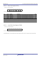
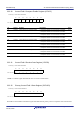
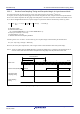
Table Of Contents
- 34. IrDA Interface
- 35. I2C-bus Interface (RIICa)
- 35.1 Overview
- 35.2 Register Descriptions
- 35.2.1 I2C-bus Control Register 1 (ICCR1)
- 35.2.2 I2C-bus Control Register 2 (ICCR2)
- 35.2.3 I2C-bus Mode Register 1 (ICMR1)
- 35.2.4 I2C-bus Mode Register 2 (ICMR2)
- 35.2.5 I2C-bus Mode Register 3 (ICMR3)
- 35.2.6 I2C-bus Function Enable Register (ICFER)
- 35.2.7 I2C-bus Status Enable Register (ICSER)
- 35.2.8 I2C-bus Interrupt Enable Register (ICIER)
- 35.2.9 I2C-bus Status Register 1 (ICSR1)
- 35.2.10 I2C-bus Status Register 2 (ICSR2)
- 35.2.11 Slave Address Register Ly (SARLy) (y = 0 to 2)
- 35.2.12 Slave Address Register Uy (SARUy) (y = 0 to 2)
- 35.2.13 I2C-bus Bit Rate Low-Level Register (ICBRL)
- 35.2.14 I2C-bus Bit Rate High-Level Register (ICBRH)
- 35.2.15 I2C-bus Transmit Data Register (ICDRT)
- 35.2.16 I2C-bus Receive Data Register (ICDRR)
- 35.2.17 I2C-bus Shift Register (ICDRS)
- 35.3 Operation
- 35.4 SCL Synchronization Circuit
- 35.5 SDA Output Delay Function
- 35.6 Digital Noise Filters
- 35.7 Address Match Detection
- 35.8 Automatic Low-Hold Function for SCL
- 35.9 Arbitration-Lost Detection Functions
- 35.10 Start Condition/Restart Condition/Stop Condition Generating Function
- 35.11 Bus Hanging
- 35.12 SMBus Operation
- 35.13 Interrupt Sources
- 35.14 Initialization of Registers and Functions When a Reset is Applied or a Condition is Detected
- 35.15 Event Link Function (Output)
- 35.16 Usage Notes
- 36. CAN Module (RSCAN)

R01UH0823EJ0110 Rev.1.10 Page 1022 of 1852
Nov 30, 2020
RX23W Group 33. Serial Communications Interface (SCIg, SCIh)
33.2.30 Control Field 0 Compare Enable Register (CF0CR)
33.2.31 Control Field 0 Receive Data Register (CF0RR)
CF0RR is a readable register that holds the value received in Control Field 0.
33.2.32 Primary Control Field 1 Data Register (PCF1DR)
PCF1DR is an 8-bit readable and writable register that holds the 8-bit primary value for comparison with Control Field 1.
Address(es): SCI12.CF0CR 0008 B32Ah
b7 b6 b5 b4 b3 b2 b1 b0
CF0CE
7
CF0CE
6
CF0CE
5
CF0CE
4
CF0CE
3
CF0CE
2
CF0CE
1
CF0CE
0
Value after reset:
00000000
Bit Symbol Bit Name Description R/W
b0 CF0CE0 Control Field 0 Bit 0 Compare Enable 0: Comparison with bit 0 of Control Field 0 is disabled.
1: Comparison with bit 0 of Control Field 0 is enabled.
R/W
b1 CF0CE1 Control Field 0 Bit 1 Compare Enable 0: Comparison with bit 1 of Control Field 0 is disabled.
1: Comparison with bit 1 of Control Field 0 is enabled.
R/W
b2 CF0CE2 Control Field 0 Bit 2 Compare Enable 0: Comparison with bit 2 of Control Field 0 is disabled.
1: Comparison with bit 2 of Control Field 0 is enabled.
R/W
b3 CF0CE3 Control Field 0 Bit 3 Compare Enable 0: Comparison with bit 3 of Control Field 0 is disabled.
1: Comparison with bit 3 of Control Field 0 is enabled.
R/W
b4 CF0CE4 Control Field 0 Bit 4 Compare Enable 0: Comparison with bit 4 of Control Field 0 is disabled.
1: Comparison with bit 4 of Control Field 0 is enabled.
R/W
b5 CF0CE5 Control Field 0 Bit 5 Compare Enable 0: Comparison with bit 5 of Control Field 0 is disabled.
1: Comparison with bit 5 of Control Field 0 is enabled.
R/W
b6 CF0CE6 Control Field 0 Bit 6 Compare Enable 0: Comparison with bit 6 of Control Field 0 is disabled.
1: Comparison with bit 6 of Control Field 0 is enabled.
R/W
b7 CF0CE7 Control Field 0 Bit 7 Compare Enable 0: Comparison with bit 7 of Control Field 0 is disabled.
1: Comparison with bit 7 of Control Field 0 is enabled.
R/W
Address(es): SCI12.CF0RR 0008 B32Bh
b7 b6 b5 b4 b3 b2 b1 b0
Value after reset:
00000000
Address(es): SCI12.PCF1DR 0008 B32Ch
b7 b6 b5 b4 b3 b2 b1 b0
Value after reset:
00000000