
Users Manual
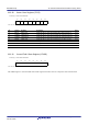
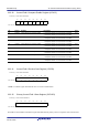
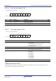
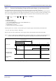
Table Of Contents
- 34. IrDA Interface
- 35. I2C-bus Interface (RIICa)
- 35.1 Overview
- 35.2 Register Descriptions
- 35.2.1 I2C-bus Control Register 1 (ICCR1)
- 35.2.2 I2C-bus Control Register 2 (ICCR2)
- 35.2.3 I2C-bus Mode Register 1 (ICMR1)
- 35.2.4 I2C-bus Mode Register 2 (ICMR2)
- 35.2.5 I2C-bus Mode Register 3 (ICMR3)
- 35.2.6 I2C-bus Function Enable Register (ICFER)
- 35.2.7 I2C-bus Status Enable Register (ICSER)
- 35.2.8 I2C-bus Interrupt Enable Register (ICIER)
- 35.2.9 I2C-bus Status Register 1 (ICSR1)
- 35.2.10 I2C-bus Status Register 2 (ICSR2)
- 35.2.11 Slave Address Register Ly (SARLy) (y = 0 to 2)
- 35.2.12 Slave Address Register Uy (SARUy) (y = 0 to 2)
- 35.2.13 I2C-bus Bit Rate Low-Level Register (ICBRL)
- 35.2.14 I2C-bus Bit Rate High-Level Register (ICBRH)
- 35.2.15 I2C-bus Transmit Data Register (ICDRT)
- 35.2.16 I2C-bus Receive Data Register (ICDRR)
- 35.2.17 I2C-bus Shift Register (ICDRS)
- 35.3 Operation
- 35.4 SCL Synchronization Circuit
- 35.5 SDA Output Delay Function
- 35.6 Digital Noise Filters
- 35.7 Address Match Detection
- 35.8 Automatic Low-Hold Function for SCL
- 35.9 Arbitration-Lost Detection Functions
- 35.10 Start Condition/Restart Condition/Stop Condition Generating Function
- 35.11 Bus Hanging
- 35.12 SMBus Operation
- 35.13 Interrupt Sources
- 35.14 Initialization of Registers and Functions When a Reset is Applied or a Condition is Detected
- 35.15 Event Link Function (Output)
- 35.16 Usage Notes
- 36. CAN Module (RSCAN)

R01UH0823EJ0110 Rev.1.10 Page 1020 of 1852
Nov 30, 2020
RX23W Group 33. Serial Communications Interface (SCIg, SCIh)
33.2.27 Status Register (STR)
Address(es): SCI12.STR 0008 B327h
b7 b6 b5 b4 b3 b2 b1 b0
— — AEDF BCDF PIBDF CF1MF CF0MF BFDF
Value after reset:
00000000
Bit Symbol Bit Name Description R/W
b0 BFDF Break Field Low Width
Detection Flag
[Setting conditions]
• Detection of the low width for a Break Field
• Completion of the output of the low width for a Break Field
• Underflow of the timer
[Clearing condition]
• Writing 1 to the STCR.BFDCL bit
R
b1 CF0MF Control Field 0 Match
Flag
[Setting condition]
• A match between the value received in Control Field 0 and the set value.
[Clearing condition]
• Writing 1 to the STCR.CF0MCL bit
R
b2 CF1MF Control Field 1 Match
Flag
[Setting condition]
• A match between the data received in Control Field 1 and the set values.
[Clearing condition]
• Writing 1 to the STCR.CF1MCL bit
R
b3 PIBDF Priority Interrupt Bit
Detection Flag
[Setting condition]
• Detection of the priority interrupt bit
[Clearing condition]
• Writing 1 to the STCR.PIBDCL bit
R
b4 BCDF Bus Collision Detected
Flag
[Setting condition]
• Detection of the bus collision
[Clearing condition]
• Writing 1 to the STCR.BCDCL bit
R
b5 AEDF Valid Edge Detection
Flag
[Setting condition]
• Detection of a valid edge
[Clearing condition]
• Writing 1 to the STCR.AEDCL bit
R
b7, b6 — Reserved These bits are read as 0. The write value should be 0. R