
Users Manual
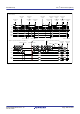

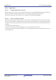
Table Of Contents
- 34. IrDA Interface
- 35. I2C-bus Interface (RIICa)
- 35.1 Overview
- 35.2 Register Descriptions
- 35.2.1 I2C-bus Control Register 1 (ICCR1)
- 35.2.2 I2C-bus Control Register 2 (ICCR2)
- 35.2.3 I2C-bus Mode Register 1 (ICMR1)
- 35.2.4 I2C-bus Mode Register 2 (ICMR2)
- 35.2.5 I2C-bus Mode Register 3 (ICMR3)
- 35.2.6 I2C-bus Function Enable Register (ICFER)
- 35.2.7 I2C-bus Status Enable Register (ICSER)
- 35.2.8 I2C-bus Interrupt Enable Register (ICIER)
- 35.2.9 I2C-bus Status Register 1 (ICSR1)
- 35.2.10 I2C-bus Status Register 2 (ICSR2)
- 35.2.11 Slave Address Register Ly (SARLy) (y = 0 to 2)
- 35.2.12 Slave Address Register Uy (SARUy) (y = 0 to 2)
- 35.2.13 I2C-bus Bit Rate Low-Level Register (ICBRL)
- 35.2.14 I2C-bus Bit Rate High-Level Register (ICBRH)
- 35.2.15 I2C-bus Transmit Data Register (ICDRT)
- 35.2.16 I2C-bus Receive Data Register (ICDRR)
- 35.2.17 I2C-bus Shift Register (ICDRS)
- 35.3 Operation
- 35.4 SCL Synchronization Circuit
- 35.5 SDA Output Delay Function
- 35.6 Digital Noise Filters
- 35.7 Address Match Detection
- 35.8 Automatic Low-Hold Function for SCL
- 35.9 Arbitration-Lost Detection Functions
- 35.10 Start Condition/Restart Condition/Stop Condition Generating Function
- 35.11 Bus Hanging
- 35.12 SMBus Operation
- 35.13 Interrupt Sources
- 35.14 Initialization of Registers and Functions When a Reset is Applied or a Condition is Detected
- 35.15 Event Link Function (Output)
- 35.16 Usage Notes
- 36. CAN Module (RSCAN)

R01UH0823EJ0110 Rev.1.10 Page 1190 of 1852
Nov 30, 2020
RX23W Group 35. I
2
C-bus Interface (RIICa)
35.11.2 Additional SCL Output Function
In master mode, the RIIC module has a facility for the output of additional SCL to release the SDA0 line from being held
low by the slave device due to the master being out of synchronization with the slave device.
This function is mainly used in master mode to release the SDA0 line from the state of being stuck low by including
additional SCL output from the RIIC with single cycles of the SCL as the unit if the RIIC cannot generate a stop
condition because the slave device is holding the SDA0 line low. Do not use this function in normal situations. Using it
when communications are proceeding correctly will lead to malfunctions.
When the ICCR1.CLO bit is set to 1, an additional clock pulse at the frequency set by the ICMR1.CKS[2:0] bits and the
ICBRH and ICBRL registers is output from the SCL0 pin. After output of this clock pulse, the CLO bit automatically
becomes 0. The SCL0 pin is held low when the ICCR2.BBSY flag is 1 and held high when the BBSY flag is 0.
Consecutive additional clock pulses can be output by writing 1 to the CLO bit after confirming the CLO bit to be 0.
When the RIIC module is in master mode and the slave device is holding the SDA0 line low because synchronization
with the slave device has been lost due to the effects of noise, etc., the output of a stop condition is not possible. The
additional SCL output function can be used to output additional clock pulses one by one to make the slave device release
the SDA0 line from being held low, thus recovering the bus from an unusable state. Release of the SDA0 line by the
slave device can be monitored by reading the ICCR1.SDAI bit. After confirming release of the SDA0 line by the slave
device, complete communications by regenerating a stop condition.
Use this function with the ICFER.MALE bit set to 0 (master arbitration-lost detection disabled).
Conditions for using the ICCR1.CLO bit
• When the bus is free (ICCR2.BBSY flag is 0) or in master mode (ICCR2.MST bit is 1 and ICCR2.BBSY flag is 1)
• When the communication device does not hold the SCL0 line low
Figure 35.40 shows the operation timing of the additional SCL output function (CLO bit).
Figure 35.40 Additional SCL Output Function (CLO Bit)
SCL0
SDA0
IICϕ
ICBRH ICBRL
9
BBSY
MST
TRS
CLO
ICBRH
ACK or Data “0”
ICBRL ICBRH ICBRL
MSB or Next Data
Data “1”
SDA line is stuck low due to irregular bits
Additional clock output Additional clock output
Write 1 to CLO bit Write 1 to CLO bit
SDA line is released
Additional SCL output
is accepted
Additional SCL output
is accepted