
Users Manual
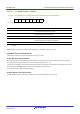
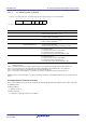
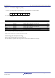
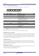
Table Of Contents
- 34. IrDA Interface
- 35. I2C-bus Interface (RIICa)
- 35.1 Overview
- 35.2 Register Descriptions
- 35.2.1 I2C-bus Control Register 1 (ICCR1)
- 35.2.2 I2C-bus Control Register 2 (ICCR2)
- 35.2.3 I2C-bus Mode Register 1 (ICMR1)
- 35.2.4 I2C-bus Mode Register 2 (ICMR2)
- 35.2.5 I2C-bus Mode Register 3 (ICMR3)
- 35.2.6 I2C-bus Function Enable Register (ICFER)
- 35.2.7 I2C-bus Status Enable Register (ICSER)
- 35.2.8 I2C-bus Interrupt Enable Register (ICIER)
- 35.2.9 I2C-bus Status Register 1 (ICSR1)
- 35.2.10 I2C-bus Status Register 2 (ICSR2)
- 35.2.11 Slave Address Register Ly (SARLy) (y = 0 to 2)
- 35.2.12 Slave Address Register Uy (SARUy) (y = 0 to 2)
- 35.2.13 I2C-bus Bit Rate Low-Level Register (ICBRL)
- 35.2.14 I2C-bus Bit Rate High-Level Register (ICBRH)
- 35.2.15 I2C-bus Transmit Data Register (ICDRT)
- 35.2.16 I2C-bus Receive Data Register (ICDRR)
- 35.2.17 I2C-bus Shift Register (ICDRS)
- 35.3 Operation
- 35.4 SCL Synchronization Circuit
- 35.5 SDA Output Delay Function
- 35.6 Digital Noise Filters
- 35.7 Address Match Detection
- 35.8 Automatic Low-Hold Function for SCL
- 35.9 Arbitration-Lost Detection Functions
- 35.10 Start Condition/Restart Condition/Stop Condition Generating Function
- 35.11 Bus Hanging
- 35.12 SMBus Operation
- 35.13 Interrupt Sources
- 35.14 Initialization of Registers and Functions When a Reset is Applied or a Condition is Detected
- 35.15 Event Link Function (Output)
- 35.16 Usage Notes
- 36. CAN Module (RSCAN)

R01UH0823EJ0110 Rev.1.10 Page 1016 of 1852
Nov 30, 2020
RX23W Group 33. Serial Communications Interface (SCIg, SCIh)
33.2.21 Control Register 0 (CR0)
33.2.22 Control Register 1 (CR1)
Address(es): SCI12.CR0 0008 B321h
b7 b6 b5 b4 b3 b2 b1 b0
————BRMERXDSFSFSF—
Value after reset:
00000000
Bit Symbol Bit Name Description R/W
b0 — Reserved This bit is read as 0. The write value should be 0. R/W
b1 SFSF Start Frame Status Flag 0: Start Frame detection function is disabled.
1: Start Frame detection function is enabled.
R
b2 RXDSF RXDX12 Input Status Flag 0: RXDX12 input is enabled.
1: RXDX12 input is disabled.
R
b3 BRME Bit Rate Measurement
Enable
0: Measurement of bit rate is disabled.
1: Measurement of bit rate is enabled.
R/W
b7 to b4 — Reserved These bits are read as 0. The write value should be 0. R/W
Address(es): SCI12.CR1 0008 B322h
b7 b6 b5 b4 b3 b2 b1 b0
PIBS[2:0] PIBE CF1DS[1:0] CF0RE BFE
Value after reset:
00000000
Bit Symbol Bit Name Description R/W
b0 BFE Break Field Enable 0: Break Field detection is disabled.
1: Break Field detection is enabled.
R/W
b1 CF0RE Control Field 0 Reception
Enable
0: Reception of Control Field 0 is disabled.
1: Reception of Control Field 0 is enabled.
R/W
b3, b2 CF1DS[1:0] Control Field 1 Data Register
Select
b3 b2
0 0: Selects comparison with the value in the PCF1DR
register.
0 1: Selects comparison with the value in the SCF1DR
register.
1 0: Selects comparison with the values in the PCF1DR and
SCF1DR registers.
1 1: Setting prohibited.
R/W
b4 PIBE Priority Interrupt Bit Enable 0: The priority interrupt bit is disabled.
1: The priority interrupt bit is enabled.
R/W
b7 to b5 PIBS[2:0] Priority Interrupt Bit Select
b7 b5
0 0 0: 0th bit of Control Field 1
0 0 1: 1st bit of Control Field 1
0 1 0: 2nd bit of Control Field 1
0 1 1: 3rd bit of Control Field 1
1 0 0: 4th bit of Control Field 1
1 0 1: 5th bit of Control Field 1
1 1 0: 6th bit of Control Field 1
1 1 1: 7th bit of Control Field 1
R/W