
Users Manual
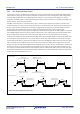
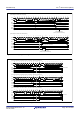
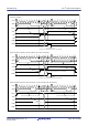
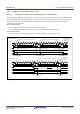
Table Of Contents
- 34. IrDA Interface
- 35. I2C-bus Interface (RIICa)
- 35.1 Overview
- 35.2 Register Descriptions
- 35.2.1 I2C-bus Control Register 1 (ICCR1)
- 35.2.2 I2C-bus Control Register 2 (ICCR2)
- 35.2.3 I2C-bus Mode Register 1 (ICMR1)
- 35.2.4 I2C-bus Mode Register 2 (ICMR2)
- 35.2.5 I2C-bus Mode Register 3 (ICMR3)
- 35.2.6 I2C-bus Function Enable Register (ICFER)
- 35.2.7 I2C-bus Status Enable Register (ICSER)
- 35.2.8 I2C-bus Interrupt Enable Register (ICIER)
- 35.2.9 I2C-bus Status Register 1 (ICSR1)
- 35.2.10 I2C-bus Status Register 2 (ICSR2)
- 35.2.11 Slave Address Register Ly (SARLy) (y = 0 to 2)
- 35.2.12 Slave Address Register Uy (SARUy) (y = 0 to 2)
- 35.2.13 I2C-bus Bit Rate Low-Level Register (ICBRL)
- 35.2.14 I2C-bus Bit Rate High-Level Register (ICBRH)
- 35.2.15 I2C-bus Transmit Data Register (ICDRT)
- 35.2.16 I2C-bus Receive Data Register (ICDRR)
- 35.2.17 I2C-bus Shift Register (ICDRS)
- 35.3 Operation
- 35.4 SCL Synchronization Circuit
- 35.5 SDA Output Delay Function
- 35.6 Digital Noise Filters
- 35.7 Address Match Detection
- 35.8 Automatic Low-Hold Function for SCL
- 35.9 Arbitration-Lost Detection Functions
- 35.10 Start Condition/Restart Condition/Stop Condition Generating Function
- 35.11 Bus Hanging
- 35.12 SMBus Operation
- 35.13 Interrupt Sources
- 35.14 Initialization of Registers and Functions When a Reset is Applied or a Condition is Detected
- 35.15 Event Link Function (Output)
- 35.16 Usage Notes
- 36. CAN Module (RSCAN)

R01UH0823EJ0110 Rev.1.10 Page 1174 of 1852
Nov 30, 2020
RX23W Group 35. I
2
C-bus Interface (RIICa)
35.7.2 Detection of the General Call Address
The RIIC also has a facility for detecting the general call address (0000 000b + 0 (write)). This is enabled by setting the
ICSER.GCAE bit to 1.
If the address following a start or restart condition is 0000 000b + 1 (read) (start byte), the RIIC recognizes this as the
address of a slave device with an “all-zero” address but not as the general call address.
When the RIIC detects the general call address, both the ICSR1.GCA flag and the ICSR2.RDRF flag are set to 1 on the
rising edge of the ninth SCL. This leads to the generation of a receive data full interrupt (RXI). The value of the GCA
flag can be confirmed to recognize that the general call address has been transmitted.
Operation after detection of the general call address is the same as normal slave receive operation.
Figure 35.27 Timing of GCA Flag Setting during Reception of General Call Address
AAS2
AAS0
S
234567
000000
1
AAS1
9
ACK
BBSY
RDRF
234567
8 9
ACK
1
General call address match (0000 000b + W)
[General call address reception]
1
0
GCA
8
W
2345
Read ICDRR register
(Dummy read [7-bit address])
Read ICDRR register
(DATA 1)
Data (DATA 1) Data (DATA 2)
Receive data (7-bit address) Receive data (DATA 1)
SCL0
SDA0