
Users Manual
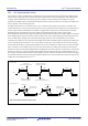
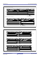
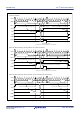
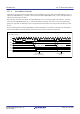
Table Of Contents
- 34. IrDA Interface
- 35. I2C-bus Interface (RIICa)
- 35.1 Overview
- 35.2 Register Descriptions
- 35.2.1 I2C-bus Control Register 1 (ICCR1)
- 35.2.2 I2C-bus Control Register 2 (ICCR2)
- 35.2.3 I2C-bus Mode Register 1 (ICMR1)
- 35.2.4 I2C-bus Mode Register 2 (ICMR2)
- 35.2.5 I2C-bus Mode Register 3 (ICMR3)
- 35.2.6 I2C-bus Function Enable Register (ICFER)
- 35.2.7 I2C-bus Status Enable Register (ICSER)
- 35.2.8 I2C-bus Interrupt Enable Register (ICIER)
- 35.2.9 I2C-bus Status Register 1 (ICSR1)
- 35.2.10 I2C-bus Status Register 2 (ICSR2)
- 35.2.11 Slave Address Register Ly (SARLy) (y = 0 to 2)
- 35.2.12 Slave Address Register Uy (SARUy) (y = 0 to 2)
- 35.2.13 I2C-bus Bit Rate Low-Level Register (ICBRL)
- 35.2.14 I2C-bus Bit Rate High-Level Register (ICBRH)
- 35.2.15 I2C-bus Transmit Data Register (ICDRT)
- 35.2.16 I2C-bus Receive Data Register (ICDRR)
- 35.2.17 I2C-bus Shift Register (ICDRS)
- 35.3 Operation
- 35.4 SCL Synchronization Circuit
- 35.5 SDA Output Delay Function
- 35.6 Digital Noise Filters
- 35.7 Address Match Detection
- 35.8 Automatic Low-Hold Function for SCL
- 35.9 Arbitration-Lost Detection Functions
- 35.10 Start Condition/Restart Condition/Stop Condition Generating Function
- 35.11 Bus Hanging
- 35.12 SMBus Operation
- 35.13 Interrupt Sources
- 35.14 Initialization of Registers and Functions When a Reset is Applied or a Condition is Detected
- 35.15 Event Link Function (Output)
- 35.16 Usage Notes
- 36. CAN Module (RSCAN)

R01UH0823EJ0110 Rev.1.10 Page 1171 of 1852
Nov 30, 2020
RX23W Group 35. I
2
C-bus Interface (RIICa)
35.6 Digital Noise Filters
The states of the SCL0 and SDA0 pins are conveyed to the internal circuitry through analog noise filters and digital noise
filters.
Figure 35.23 is a block diagram of the digital noise filter.
The on-chip digital noise filter of each RIIC consists of four flip-flop circuit stages connected in series and a match
detection circuit.
The number of effective stages in the digital noise filter is selected by the ICMR3.NF[1:0] bits. The selected number of
effective stages determines the noise-filtering capability as a period from one to four cycles of IICφ.
The input signal to the SCL0 pin (or SDA0 pin) is sampled on falling edges of the IICφ signal. When the input signal
level matches the output level for the number of effective flip-flop circuit stages selected by the ICMR3.NF[1:0] bits, the
signal level is conveyed to the subsequent stages. If the signal levels do not match, the previous value is retained.
If the ratio between the frequency of the internal operating clock (PCLK) and the transfer rate is relatively small (e.g.
data transfer at 400 kbps with PCLK = 4 MHz), the characteristics of the digital noise filter may lead to the elimination
of needed signals as noise. In such cases, it is possible to disable the digital noise filter (by setting the ICFER.NFE bit to
0) and use only the analog noise filter.
Figure 35.23 Block Diagram of the Digital Noise Filter
Mismatch
Match
NFE : Digital noise filter enable bit
NF[1:0] : Noise filter stage select bits
Q
T
D
Q
T
D
Q
T
D
Q
T
D
Q
T
D
IICϕ
Four-stage digital noise filter
NF[1:0] NFE
Com-
parator
Q
T
D
PCLK
SCL0/SDA0
input signal
SCL0/SDA0
internal signal