
Users Manual
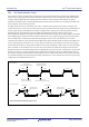
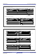
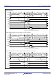
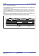
Table Of Contents
- 34. IrDA Interface
- 35. I2C-bus Interface (RIICa)
- 35.1 Overview
- 35.2 Register Descriptions
- 35.2.1 I2C-bus Control Register 1 (ICCR1)
- 35.2.2 I2C-bus Control Register 2 (ICCR2)
- 35.2.3 I2C-bus Mode Register 1 (ICMR1)
- 35.2.4 I2C-bus Mode Register 2 (ICMR2)
- 35.2.5 I2C-bus Mode Register 3 (ICMR3)
- 35.2.6 I2C-bus Function Enable Register (ICFER)
- 35.2.7 I2C-bus Status Enable Register (ICSER)
- 35.2.8 I2C-bus Interrupt Enable Register (ICIER)
- 35.2.9 I2C-bus Status Register 1 (ICSR1)
- 35.2.10 I2C-bus Status Register 2 (ICSR2)
- 35.2.11 Slave Address Register Ly (SARLy) (y = 0 to 2)
- 35.2.12 Slave Address Register Uy (SARUy) (y = 0 to 2)
- 35.2.13 I2C-bus Bit Rate Low-Level Register (ICBRL)
- 35.2.14 I2C-bus Bit Rate High-Level Register (ICBRH)
- 35.2.15 I2C-bus Transmit Data Register (ICDRT)
- 35.2.16 I2C-bus Receive Data Register (ICDRR)
- 35.2.17 I2C-bus Shift Register (ICDRS)
- 35.3 Operation
- 35.4 SCL Synchronization Circuit
- 35.5 SDA Output Delay Function
- 35.6 Digital Noise Filters
- 35.7 Address Match Detection
- 35.8 Automatic Low-Hold Function for SCL
- 35.9 Arbitration-Lost Detection Functions
- 35.10 Start Condition/Restart Condition/Stop Condition Generating Function
- 35.11 Bus Hanging
- 35.12 SMBus Operation
- 35.13 Interrupt Sources
- 35.14 Initialization of Registers and Functions When a Reset is Applied or a Condition is Detected
- 35.15 Event Link Function (Output)
- 35.16 Usage Notes
- 36. CAN Module (RSCAN)

R01UH0823EJ0110 Rev.1.10 Page 1170 of 1852
Nov 30, 2020
RX23W Group 35. I
2
C-bus Interface (RIICa)
35.5 SDA Output Delay Function
The RIIC module incorporates a function for delaying output on the SDA line. The delay can be applied to all output
(generation of the start, restart, and stop conditions, data, and the ACK and NACK signals) on the SDA line.
The SDA output delay function is used to delay the SDA output timing relative to falling edges of SCL to ensure that the
SDA signal changes while the SCL is low and can be used to prevent erroneous operation of communications devices.
This function is also used to satisfy the 300 ns (min.) data hold time prescribed by the SMBus specification.
The output delay function is enabled by setting the ICMR2.SDDL[2:0] bits to any value other than 000b, and disabled by
setting the same bits to 000b.
When the SDA output delay function is enabled (the SDDL[2:0] bits are not “000b”), the SDA output delay counter
counts the number of cycles set in the SDDL[2:0] bits of the count source selected by the ICMR2.DLCS bit (the internal
reference clock (IICφ) or internal reference clock divided by 2 (IICφ/2)). On completion of counting of cycles of delay,
the RIIC changes the bit being output as the SDA signal (generation of the start, restart, or stop condition, a new bit, or an
ACK or NACK signal).
Figure 35.22 SDA Output Delay Function
SDA output delay
b6 to b0
1 to 9
SDA output delay
b7 to b1
1 to 7
SDA output release timing
Master mode
Receive mode
ST RS SP1 2 to 8 9
ICBRH ICBRL ICBRH ICBRL
ICBRH
ACK/NACKb7
ST
BBSY
8
b7 to b1
89
b0
S 9
P
Transmit mode
SDA output delay
ACK/NACK
b0
SDA output release timing
*
1
ACK/NACK
ICBRL ICBRH ICBRLICBRL
*
1
Analog noise filter delay time + PCLK sampling error (1 PCLK (max))
Digital noise filter delay time (NFE bit, NF[1:0] bits settings = 0.5 PCLK (min), 1 IICϕ to 4 IICϕ (max))
SDA output delay time (DLCS bit, SDDL[2:0] bits settings = 0 (min) to 14 IICϕ (max))
*
1
Note 1. The output delay function is set by the DLCS and SDDL[2:0] bits when a start (ST),
restart (RS), or stop (SP) condition is generated.
SCL0
SDA0
SCL0
SDA0
SCL0
SDA0