
Users Manual
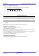
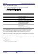
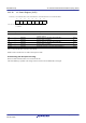
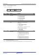
Table Of Contents
- 34. IrDA Interface
- 35. I2C-bus Interface (RIICa)
- 35.1 Overview
- 35.2 Register Descriptions
- 35.2.1 I2C-bus Control Register 1 (ICCR1)
- 35.2.2 I2C-bus Control Register 2 (ICCR2)
- 35.2.3 I2C-bus Mode Register 1 (ICMR1)
- 35.2.4 I2C-bus Mode Register 2 (ICMR2)
- 35.2.5 I2C-bus Mode Register 3 (ICMR3)
- 35.2.6 I2C-bus Function Enable Register (ICFER)
- 35.2.7 I2C-bus Status Enable Register (ICSER)
- 35.2.8 I2C-bus Interrupt Enable Register (ICIER)
- 35.2.9 I2C-bus Status Register 1 (ICSR1)
- 35.2.10 I2C-bus Status Register 2 (ICSR2)
- 35.2.11 Slave Address Register Ly (SARLy) (y = 0 to 2)
- 35.2.12 Slave Address Register Uy (SARUy) (y = 0 to 2)
- 35.2.13 I2C-bus Bit Rate Low-Level Register (ICBRL)
- 35.2.14 I2C-bus Bit Rate High-Level Register (ICBRH)
- 35.2.15 I2C-bus Transmit Data Register (ICDRT)
- 35.2.16 I2C-bus Receive Data Register (ICDRR)
- 35.2.17 I2C-bus Shift Register (ICDRS)
- 35.3 Operation
- 35.4 SCL Synchronization Circuit
- 35.5 SDA Output Delay Function
- 35.6 Digital Noise Filters
- 35.7 Address Match Detection
- 35.8 Automatic Low-Hold Function for SCL
- 35.9 Arbitration-Lost Detection Functions
- 35.10 Start Condition/Restart Condition/Stop Condition Generating Function
- 35.11 Bus Hanging
- 35.12 SMBus Operation
- 35.13 Interrupt Sources
- 35.14 Initialization of Registers and Functions When a Reset is Applied or a Condition is Detected
- 35.15 Event Link Function (Output)
- 35.16 Usage Notes
- 36. CAN Module (RSCAN)

R01UH0823EJ0110 Rev.1.10 Page 1015 of 1852
Nov 30, 2020
RX23W Group 33. Serial Communications Interface (SCIg, SCIh)
MFF Flag (Mode Fault Flag)
This bit indicates mode fault errors.
In a multi-master configuration, determine the mode fault error occurrence by reading the MFF flag.
[Setting condition]
• Input on the SSn# pin being at the low level during master operation in simple SPI mode (SSE bit = 1 and MSS bit
= 0)
[Clearing condition]
• Writing 0 to the bit after it was read as 1
CKPOL Bit (Clock Polarity Select)
This bit selects the polarity of the clock signal output through the SCKn pin. Refer to
Figure 33.58 for details.
Set the bit to 0 in other than simple SPI mode and clock synchronous mode.
CKPH Bit (Clock Phase Select)
This bit selects the phase of the clock signal output through the SCKn pin. Refer to
Figure 33.58 for details.
Set the bit to 0 in other than simple SPI mode and clock synchronous mode.
33.2.20 Extended Serial Module Enable Register (ESMER)
ESME Bit (Extended Serial Mode Enable)
When the ESME bit is 1, the facilities of the extended serial mode control section are enabled.
When the ESME bit is 0, the extended serial mode control section is initialized.
Note 1. Operation is only possible with PCLK selected.
Address(es): SCI12.ESMER 0008 B320h
b7 b6 b5 b4 b3 b2 b1 b0
———————ESME
Value after reset:
00000000
Bit Symbol Bit Name Description R/W
b0 ESME Extended Serial Mode
Enable
0: The extended serial mode is disabled.
1: The extended serial mode is enabled.
R/W
b7 to b1 — Reserved These bits are read as 0. The write value should be 0. R/W
Table 33.26 Settings of the ESME Bit and Timer Operation Mode
ESME Bit Timer Mode Break Field Low Width Determination Mode Break Field Low Width Output Mode
0 Available*
1
Not available Not available
1 Available Available Available