
Users Manual
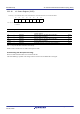
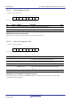
Table Of Contents
- 34. IrDA Interface
- 35. I2C-bus Interface (RIICa)
- 35.1 Overview
- 35.2 Register Descriptions
- 35.2.1 I2C-bus Control Register 1 (ICCR1)
- 35.2.2 I2C-bus Control Register 2 (ICCR2)
- 35.2.3 I2C-bus Mode Register 1 (ICMR1)
- 35.2.4 I2C-bus Mode Register 2 (ICMR2)
- 35.2.5 I2C-bus Mode Register 3 (ICMR3)
- 35.2.6 I2C-bus Function Enable Register (ICFER)
- 35.2.7 I2C-bus Status Enable Register (ICSER)
- 35.2.8 I2C-bus Interrupt Enable Register (ICIER)
- 35.2.9 I2C-bus Status Register 1 (ICSR1)
- 35.2.10 I2C-bus Status Register 2 (ICSR2)
- 35.2.11 Slave Address Register Ly (SARLy) (y = 0 to 2)
- 35.2.12 Slave Address Register Uy (SARUy) (y = 0 to 2)
- 35.2.13 I2C-bus Bit Rate Low-Level Register (ICBRL)
- 35.2.14 I2C-bus Bit Rate High-Level Register (ICBRH)
- 35.2.15 I2C-bus Transmit Data Register (ICDRT)
- 35.2.16 I2C-bus Receive Data Register (ICDRR)
- 35.2.17 I2C-bus Shift Register (ICDRS)
- 35.3 Operation
- 35.4 SCL Synchronization Circuit
- 35.5 SDA Output Delay Function
- 35.6 Digital Noise Filters
- 35.7 Address Match Detection
- 35.8 Automatic Low-Hold Function for SCL
- 35.9 Arbitration-Lost Detection Functions
- 35.10 Start Condition/Restart Condition/Stop Condition Generating Function
- 35.11 Bus Hanging
- 35.12 SMBus Operation
- 35.13 Interrupt Sources
- 35.14 Initialization of Registers and Functions When a Reset is Applied or a Condition is Detected
- 35.15 Event Link Function (Output)
- 35.16 Usage Notes
- 36. CAN Module (RSCAN)

R01UH0823EJ0110 Rev.1.10 Page 1013 of 1852
Nov 30, 2020
RX23W Group 33. Serial Communications Interface (SCIg, SCIh)
33.2.18 I
2
C Status Register (SISR)
Note 1. Only 0 can be written to this bit, to clear the flag.
SISR is used to monitor state in relation to simple I
2
C mode.
IICACKR Flag (ACK Reception Data Flag)
Received ACK and NACK bits can be read from this bit.
The IICACKR flag is updated at the rising of SSCLn clock for the ACK/NACK receiving bit.
Address(es): SCI1.SISR 0008 A02Ch, SCI5.SISR 0008 A0ACh, SCI8.SISR 0008 A10Ch, SCI12.SISR 0008 B30Ch
b7 b6 b5 b4 b3 b2 b1 b0
———————
IICACK
R
Value after reset:
00xx0x00
x: Undefined
Bit Symbol Bit Name Description R/W
b0 IICACKR ACK Reception Data Flag 0: ACK received
1: NACK received
R/W*
1
b1 — Reserved This bit is read as 0. The write value should be 0. R/W
b2 — Reserved The read value is undefined. R
b3 — Reserved This bit is read as 0. The write value should be 0. R/W
b5, b4 — Reserved The read value is undefined. R
b7, b6 — Reserved These bits are read as 0. The write value should be 0. R/W