
Users Manual
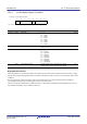
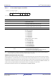
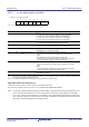
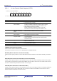
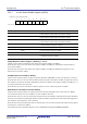
Table Of Contents
- 34. IrDA Interface
- 35. I2C-bus Interface (RIICa)
- 35.1 Overview
- 35.2 Register Descriptions
- 35.2.1 I2C-bus Control Register 1 (ICCR1)
- 35.2.2 I2C-bus Control Register 2 (ICCR2)
- 35.2.3 I2C-bus Mode Register 1 (ICMR1)
- 35.2.4 I2C-bus Mode Register 2 (ICMR2)
- 35.2.5 I2C-bus Mode Register 3 (ICMR3)
- 35.2.6 I2C-bus Function Enable Register (ICFER)
- 35.2.7 I2C-bus Status Enable Register (ICSER)
- 35.2.8 I2C-bus Interrupt Enable Register (ICIER)
- 35.2.9 I2C-bus Status Register 1 (ICSR1)
- 35.2.10 I2C-bus Status Register 2 (ICSR2)
- 35.2.11 Slave Address Register Ly (SARLy) (y = 0 to 2)
- 35.2.12 Slave Address Register Uy (SARUy) (y = 0 to 2)
- 35.2.13 I2C-bus Bit Rate Low-Level Register (ICBRL)
- 35.2.14 I2C-bus Bit Rate High-Level Register (ICBRH)
- 35.2.15 I2C-bus Transmit Data Register (ICDRT)
- 35.2.16 I2C-bus Receive Data Register (ICDRR)
- 35.2.17 I2C-bus Shift Register (ICDRS)
- 35.3 Operation
- 35.4 SCL Synchronization Circuit
- 35.5 SDA Output Delay Function
- 35.6 Digital Noise Filters
- 35.7 Address Match Detection
- 35.8 Automatic Low-Hold Function for SCL
- 35.9 Arbitration-Lost Detection Functions
- 35.10 Start Condition/Restart Condition/Stop Condition Generating Function
- 35.11 Bus Hanging
- 35.12 SMBus Operation
- 35.13 Interrupt Sources
- 35.14 Initialization of Registers and Functions When a Reset is Applied or a Condition is Detected
- 35.15 Event Link Function (Output)
- 35.16 Usage Notes
- 36. CAN Module (RSCAN)

R01UH0823EJ0110 Rev.1.10 Page 1130 of 1852
Nov 30, 2020
RX23W Group 35. I
2
C-bus Interface (RIICa)
35.2.3 I
2
C-bus Mode Register 1 (ICMR1)
Note 1. Rewrite the BC[2:0] bits and set the BCWP bit to 0 at the same time.
BC[2:0] Bits (Bit Counter)
These bits function as a counter that indicates the number of bits remaining to be transferred at the detection of a rising
edge on the SCL0 line. Although these bits are writable and readable, it is not necessary to access these bits under normal
conditions.
To write to these bits, specify the number of bits to be transferred plus one (data is transferred with an additional
acknowledgment bit) between transferred bytes when the SCL0 line is low.
The values of the BC[2:0] bits return to 000b at the end of a data transfer including the acknowledgment bit or when a
start condition including a restart condition is detected.
Address(es): RIIC0.ICMR1 0008 8302h
b7 b6 b5 b4 b3 b2 b1 b0
MTWP CKS[2:0] BCWP BC[2:0]
Value after reset:
00001000
Bit Symbol Bit Name Description R/W
b2 to b0 BC[2:0] Bit Counter
b2 b0
0 0 0: 9 bits
0 0 1: 2 bits
0 1 0: 3 bits
0 1 1: 4 bits
1 0 0: 5 bits
1 0 1: 6 bits
1 1 0: 7 bits
1 1 1: 8 bits
R/W*
1
b3 BCWP BC Write Protect 0: Enables a value to be written in the BC[2:0] bits.
(This bit is read as 1.)
R/W*
1
b6 to b4 CKS[2:0] Internal Reference Clock Select Select the internal reference clock (IICφ) source for the RIIC.
b6 b4
0 0 0: PCLK/1
0 0 1: PCLK/2
0 1 0: PCLK/4
0 1 1: PCLK/8
1 0 0: PCLK/16
1 0 1: PCLK/32
1 1 0: PCLK/64
1 1 1: PCLK/128
R/W
b7 MTWP MST/TRS Write Protect 0: Disables writing to the ICCR2.MST and TRS bits.
1: Enables writing to the ICCR2.MST and TRS bits.
R/W