
Users Manual
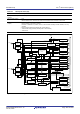
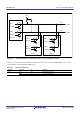
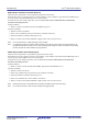
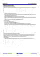
Table Of Contents
- 34. IrDA Interface
- 35. I2C-bus Interface (RIICa)
- 35.1 Overview
- 35.2 Register Descriptions
- 35.2.1 I2C-bus Control Register 1 (ICCR1)
- 35.2.2 I2C-bus Control Register 2 (ICCR2)
- 35.2.3 I2C-bus Mode Register 1 (ICMR1)
- 35.2.4 I2C-bus Mode Register 2 (ICMR2)
- 35.2.5 I2C-bus Mode Register 3 (ICMR3)
- 35.2.6 I2C-bus Function Enable Register (ICFER)
- 35.2.7 I2C-bus Status Enable Register (ICSER)
- 35.2.8 I2C-bus Interrupt Enable Register (ICIER)
- 35.2.9 I2C-bus Status Register 1 (ICSR1)
- 35.2.10 I2C-bus Status Register 2 (ICSR2)
- 35.2.11 Slave Address Register Ly (SARLy) (y = 0 to 2)
- 35.2.12 Slave Address Register Uy (SARUy) (y = 0 to 2)
- 35.2.13 I2C-bus Bit Rate Low-Level Register (ICBRL)
- 35.2.14 I2C-bus Bit Rate High-Level Register (ICBRH)
- 35.2.15 I2C-bus Transmit Data Register (ICDRT)
- 35.2.16 I2C-bus Receive Data Register (ICDRR)
- 35.2.17 I2C-bus Shift Register (ICDRS)
- 35.3 Operation
- 35.4 SCL Synchronization Circuit
- 35.5 SDA Output Delay Function
- 35.6 Digital Noise Filters
- 35.7 Address Match Detection
- 35.8 Automatic Low-Hold Function for SCL
- 35.9 Arbitration-Lost Detection Functions
- 35.10 Start Condition/Restart Condition/Stop Condition Generating Function
- 35.11 Bus Hanging
- 35.12 SMBus Operation
- 35.13 Interrupt Sources
- 35.14 Initialization of Registers and Functions When a Reset is Applied or a Condition is Detected
- 35.15 Event Link Function (Output)
- 35.16 Usage Notes
- 36. CAN Module (RSCAN)

R01UH0823EJ0110 Rev.1.10 Page 1122 of 1852
Nov 30, 2020
RX23W Group 35. I
2
C-bus Interface (RIICa)
Figure 35.1 RIIC Block Diagram
Low power consumption
function
Module stop state can be set.
RIIC operating modes
• Four
Master transmit mode, master receive mode, slave transmit mode, and slave receive mode
Event link function
(output)
• Four sources (RIIC0):
Error in transfer or occurrence of events
Detection of arbitration-lost, NACK, timeout, a start condition including a restart condition, or a stop
condition
• Receive data full (including matching with a slave address)
• Transmit data empty (including matching with a slave address)
• Transmit end
Table 35.1 RIIC Specifications (2/2)
Item Description
ICCR1
Output
control
Noise
canceller
Bus state decision
circuit
Arbitration decision
circuit
Output
control
Noise
canceller
ICDRS
ICDRT
ICDRR
Address comparator
ICCR2
ICMR1
ICMR2
ICMR3
ICFER
ICSR1
ICSR2
ICSER
ICIER
ICBRH
ICBRL
Timeout circuit
Interrupt generator
Transmission/
reception control
circuit
Transfer clock
generator
ACK output circuit
SCL0
SDA0
NACK decision/ACK
reception circuit
Internal peripheral bus
BC[2:0]
CKS[2:0]
CLO
SDAI
BBSY, MST, TRS
SDA output delay control
ST, RS, SP
IICRST
SDDL[2:0]
PCLK
ACKBR
WAIT, RDRFS
NF[1:0]
ACKBT
NFE
SARL0
SARL1
SARL2
SARU0
SARU1
SARU2
NACKF
Interrupt request
(TXI, TEI, RXI, EEI)
NF[1:0]
NFE
MALE, NALE, SALE
TMOE TMOS, TMOH, TMOL
SCLE
NACKE
SCLI
SCLO, SDAO
PS
DLCS
TMOF
PS
IICϕ (PCLK/1 to PCLK/128)
IICϕ, IICϕ/2
Event output