
Users Manual
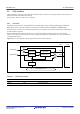
Table Of Contents
- 34. IrDA Interface
- 35. I2C-bus Interface (RIICa)
- 35.1 Overview
- 35.2 Register Descriptions
- 35.2.1 I2C-bus Control Register 1 (ICCR1)
- 35.2.2 I2C-bus Control Register 2 (ICCR2)
- 35.2.3 I2C-bus Mode Register 1 (ICMR1)
- 35.2.4 I2C-bus Mode Register 2 (ICMR2)
- 35.2.5 I2C-bus Mode Register 3 (ICMR3)
- 35.2.6 I2C-bus Function Enable Register (ICFER)
- 35.2.7 I2C-bus Status Enable Register (ICSER)
- 35.2.8 I2C-bus Interrupt Enable Register (ICIER)
- 35.2.9 I2C-bus Status Register 1 (ICSR1)
- 35.2.10 I2C-bus Status Register 2 (ICSR2)
- 35.2.11 Slave Address Register Ly (SARLy) (y = 0 to 2)
- 35.2.12 Slave Address Register Uy (SARUy) (y = 0 to 2)
- 35.2.13 I2C-bus Bit Rate Low-Level Register (ICBRL)
- 35.2.14 I2C-bus Bit Rate High-Level Register (ICBRH)
- 35.2.15 I2C-bus Transmit Data Register (ICDRT)
- 35.2.16 I2C-bus Receive Data Register (ICDRR)
- 35.2.17 I2C-bus Shift Register (ICDRS)
- 35.3 Operation
- 35.4 SCL Synchronization Circuit
- 35.5 SDA Output Delay Function
- 35.6 Digital Noise Filters
- 35.7 Address Match Detection
- 35.8 Automatic Low-Hold Function for SCL
- 35.9 Arbitration-Lost Detection Functions
- 35.10 Start Condition/Restart Condition/Stop Condition Generating Function
- 35.11 Bus Hanging
- 35.12 SMBus Operation
- 35.13 Interrupt Sources
- 35.14 Initialization of Registers and Functions When a Reset is Applied or a Condition is Detected
- 35.15 Event Link Function (Output)
- 35.16 Usage Notes
- 36. CAN Module (RSCAN)

R01UH0823EJ0110 Rev.1.10 Page 1114 of 1852
Nov 30, 2020
RX23W Group 33. Serial Communications Interface (SCIg, SCIh)
33.14.14 Note on Transmit Enable Bit (TE Bit)
When setting the pin function to “TXDn” while the SCR.TE bit is 0 (serial transmission is disabled) or setting the TE bit
to 0 while the pin function is “TXDn”, output of the TXDn pin becomes high-impedance.
Prevent the TXDn line from becoming high-impedance by any of the following ways:
(1) Connect a pull-up resistor to the TXDn line.
(2) Set the TE bit to 1
*
1
before changing the pin function to “TXDn”. Change the pin function to “general-purpose I/O
port, output” before setting the TE bit to 0.
Note 1. An interrupt is generated when the TE bit is set to 1 while the TXI interrupt is enabled. If this creates a problem,
change the pin function to “TXDn” first, and then set the corresponding ICU.IERm.IENj bit to 1.
33.14.15 Note on Stopping Reception When Using the RTS Function in Asynchronous
Mode
One clock cycle of PCLK is required for the time from setting the SCR.RE bit to 0 to stopping the RTS signal generator
in asynchronous mode.
When reading the RDR (or RDRL) register after setting the SCR.RE bit to 0, confirm that the RE bit has been set to 0
before reading the RDR (or RDRL) register to prevent these two processes from being performed consecutively.