
Users Manual
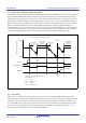
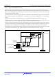
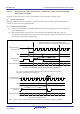
Table Of Contents
- 34. IrDA Interface
- 35. I2C-bus Interface (RIICa)
- 35.1 Overview
- 35.2 Register Descriptions
- 35.2.1 I2C-bus Control Register 1 (ICCR1)
- 35.2.2 I2C-bus Control Register 2 (ICCR2)
- 35.2.3 I2C-bus Mode Register 1 (ICMR1)
- 35.2.4 I2C-bus Mode Register 2 (ICMR2)
- 35.2.5 I2C-bus Mode Register 3 (ICMR3)
- 35.2.6 I2C-bus Function Enable Register (ICFER)
- 35.2.7 I2C-bus Status Enable Register (ICSER)
- 35.2.8 I2C-bus Interrupt Enable Register (ICIER)
- 35.2.9 I2C-bus Status Register 1 (ICSR1)
- 35.2.10 I2C-bus Status Register 2 (ICSR2)
- 35.2.11 Slave Address Register Ly (SARLy) (y = 0 to 2)
- 35.2.12 Slave Address Register Uy (SARUy) (y = 0 to 2)
- 35.2.13 I2C-bus Bit Rate Low-Level Register (ICBRL)
- 35.2.14 I2C-bus Bit Rate High-Level Register (ICBRH)
- 35.2.15 I2C-bus Transmit Data Register (ICDRT)
- 35.2.16 I2C-bus Receive Data Register (ICDRR)
- 35.2.17 I2C-bus Shift Register (ICDRS)
- 35.3 Operation
- 35.4 SCL Synchronization Circuit
- 35.5 SDA Output Delay Function
- 35.6 Digital Noise Filters
- 35.7 Address Match Detection
- 35.8 Automatic Low-Hold Function for SCL
- 35.9 Arbitration-Lost Detection Functions
- 35.10 Start Condition/Restart Condition/Stop Condition Generating Function
- 35.11 Bus Hanging
- 35.12 SMBus Operation
- 35.13 Interrupt Sources
- 35.14 Initialization of Registers and Functions When a Reset is Applied or a Condition is Detected
- 35.15 Event Link Function (Output)
- 35.16 Usage Notes
- 36. CAN Module (RSCAN)

R01UH0823EJ0110 Rev.1.10 Page 1108 of 1852
Nov 30, 2020
RX23W Group 33. Serial Communications Interface (SCIg, SCIh)
33.14.7 Restrictions on Using DMAC or DTC
When using the DMAC or DTC to read the RDR, RDRH, and RDRL registers, be sure to set the receive data full
interrupt (RXI) as the activation source of the relevant SCI.
33.14.8 Notes on Starting Transfer
At the point where transfer starts when the interrupt status flag (IRn.IR flag) in the interrupt controller is 1, follow the
procedure below to clear interrupt requests before permitting operations (by setting the SCR.TE or SCR.RE bit to 1). For
details on the interrupt status flag, refer to
section 15, Interrupt Controller (ICUb).
• Confirm that transfer has stopped (the setting of the SCR.TE or SCR.RE bits is 0).
• Set the corresponding interrupt enable bit (SCR.TIE or SCR.RIE) to 0.
• Read the corresponding interrupt enable bit (SCR.TIE or SCR.RIE bit) to check that it has become 0.
• Set the interrupt status flag (IRn.IR flag) in the interrupt controller to 0.
33.14.9 SCI Operations during Low Power Consumption State
(1) Transmission
When making settings for the module stopped state or in transitions to software standby, stop operations (by setting the
TIE, TE, and TEIE bits in the SCR register to 0) after switching the TXDn pin to the general I/O port pin function.
Setting the TE bit to 0 resets the TSR register and the SSR.TEND flag. Depending on the port settings, output pins may
output the level before a transition to the low power consumption state is made after release from the module stopped
state or software standby mode. When transitions to these states are made during transmission, the data being transmitted
become indeterminate.
To transmit data in the same transmit mode after cancellation of the low power consumption state, set the TE bit to 1,
read the SSR register, and write data to the TDR register sequentially to start data transmission. To transmit data with a
different transmit mode, initialize the SCI first.
Figure 33.77 shows a sample flowchart for transition to software standby mode during transmission. Figure 33.78 and
Figure 33.79 show the port pin states during transition to software standby mode.
Before specifying the module stop state or making a transition to software standby mode from the transmit mode using
DTC/DMA transfer, stop the transmit operations (TE = 0). To start transmission after cancellation using the DTC/
DMAC, set the TE and TIE bits to 1. The TXI interrupt flag is set to 1 and transmission starts using the DTC/DMAC.
(2) Reception
Before specifying the module stop state or making a transition to software standby mode, stop the receive operations
(SCR.RE = 0). If transition is made during data reception, the data being received will be invalid.
To receive data in the same receive mode after cancellation of the low power consumption state, set the RE bit to 1, and
then start reception. To receive data in a different receive mode, initialize the SCI first.
Figure 33.80 shows a sample flowchart for transition to software standby mode during reception.