
Users Manual
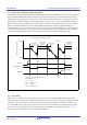
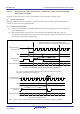
Table Of Contents
- 34. IrDA Interface
- 35. I2C-bus Interface (RIICa)
- 35.1 Overview
- 35.2 Register Descriptions
- 35.2.1 I2C-bus Control Register 1 (ICCR1)
- 35.2.2 I2C-bus Control Register 2 (ICCR2)
- 35.2.3 I2C-bus Mode Register 1 (ICMR1)
- 35.2.4 I2C-bus Mode Register 2 (ICMR2)
- 35.2.5 I2C-bus Mode Register 3 (ICMR3)
- 35.2.6 I2C-bus Function Enable Register (ICFER)
- 35.2.7 I2C-bus Status Enable Register (ICSER)
- 35.2.8 I2C-bus Interrupt Enable Register (ICIER)
- 35.2.9 I2C-bus Status Register 1 (ICSR1)
- 35.2.10 I2C-bus Status Register 2 (ICSR2)
- 35.2.11 Slave Address Register Ly (SARLy) (y = 0 to 2)
- 35.2.12 Slave Address Register Uy (SARUy) (y = 0 to 2)
- 35.2.13 I2C-bus Bit Rate Low-Level Register (ICBRL)
- 35.2.14 I2C-bus Bit Rate High-Level Register (ICBRH)
- 35.2.15 I2C-bus Transmit Data Register (ICDRT)
- 35.2.16 I2C-bus Receive Data Register (ICDRR)
- 35.2.17 I2C-bus Shift Register (ICDRS)
- 35.3 Operation
- 35.4 SCL Synchronization Circuit
- 35.5 SDA Output Delay Function
- 35.6 Digital Noise Filters
- 35.7 Address Match Detection
- 35.8 Automatic Low-Hold Function for SCL
- 35.9 Arbitration-Lost Detection Functions
- 35.10 Start Condition/Restart Condition/Stop Condition Generating Function
- 35.11 Bus Hanging
- 35.12 SMBus Operation
- 35.13 Interrupt Sources
- 35.14 Initialization of Registers and Functions When a Reset is Applied or a Condition is Detected
- 35.15 Event Link Function (Output)
- 35.16 Usage Notes
- 36. CAN Module (RSCAN)

R01UH0823EJ0110 Rev.1.10 Page 1106 of 1852
Nov 30, 2020
RX23W Group 33. Serial Communications Interface (SCIg, SCIh)
33.14 Usage Notes
33.14.1 Setting the Module Stop Function
Module stop control register B (MSTPCRB) and module stop control register C (MSTPCRC) are used to stop and start
SCI operations. With the value after a reset, SCI operations are stopped. Register access is enabled by releasing the
module stop state. For details, refer to
section 11, Low Power Consumption.
33.14.2 Break Detection and Processing
When a framing error is detected, a break can be detected by reading the RXDn pin value directly. In a break, the input
from the RXDn pin becomes all 0s, and so the SSR.FER flag is set to 1 (framing error has occurred), and the SSR.PER
flag may also be set to 1 (parity error has occurred). When the SEMR.RXDESEL bit is 0, the SCI continues the receive
operation even after a break is received. Therefore, note that even if the FER flag is set to 0 (no framing error occurred),
it will be set to 1 again. When the SEMR.RXDESEL bit is 1, the SCI sets the SSR.FER flag to 1 and stops receiving
operation until a start bit of the next data frame is detected. If the SSR.FER flag is set to 0 at this time, the SSR.FER flag
retains 0 during the break. When the RXDn pin becomes high and the break ends, detecting the beginning of the start bit
at the first falling edge of the RXDn pin allows the SCI to start the receiving operation.
33.14.3 Mark State and Sending Breaks
When the SCR.TE bit is 0 (serial transmission is disabled), the TXDn pin becomes high-impedance. To forcibly set the
TXDn pin to mark or space state while the TE bit is 0, set the I/O port associated registers and switch the TXDn pin to
general output port.
For holding the communication line in the mark (“1”) state until the TE bit is set to 1 (serial transmission is enabled), set
the corresponding bit in the PODR register to 1 for high output from general output port. To start communications, set the
TE bit to 1 and then the corresponding bit in the PMR register to 1.
To send a break (the space state for longer than a certain period of time) while data transmission, set the corresponding
bit in the PODR register to 0 (low output), and set the corresponding bit in the PMR register to 0 (general I/O port). Then
set the TE bit to 0 if necessary. When the TE bit is set to 0, the transmitter is initialized regardless of the current transmit
status.
33.14.4 Receive Error Flags and Transmit Operations (Clock Synchronous Mode and
Simple SPI Mode)
Transmission cannot be started when a receive error flag (SSR.ORER) is set to 1, even if data is written to the TDR
register. Be sure to set the receive error flags to 0 before starting transmission. Note also that the receive error flags
cannot be set to 0 even if the SCR.RE bit is set to 0 (serial reception is disabled).
33.14.5 Writing Data to the TDR Register
Data can be written to registers TDR, TDRH, and TDRL. However, if new data is written to registers TDR, TDRH, and
TDRL when transmit data is remaining in registers TDR, TDRH, and TDRL, the previous data in registers TDR, TDRH,
and TDRL is lost because it has not been transferred to the TSR register yet. Be sure to write transmit data to registers
TDR, TDRH, and TDRL in the TXI interrupt request handling routine.