
User's Manual
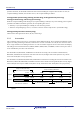
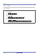

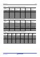
Table Of Contents
- Cover
- Notice
- General Precautions in the Handling of Microprocessing Unit and Microcontroller Unit Products
- How to Use This Manual
- Contents
- Features
- 1. Overview
- 2. CPU
- 2.1 Features
- 2.2 Register Set of the CPU
- 2.2.1 General-Purpose Registers (R0 to R15)
- 2.2.2 Control Registers
- 2.2.2.1 Interrupt Stack Pointer (ISP)/User Stack Pointer (USP)
- 2.2.2.2 Exception Table Register (EXTB)
- 2.2.2.3 Interrupt Table Register (INTB)
- 2.2.2.4 Program Counter (PC)
- 2.2.2.5 Processor Status Word (PSW)
- 2.2.2.6 Backup PC (BPC)
- 2.2.2.7 Backup PSW (BPSW)
- 2.2.2.8 Fast Interrupt Vector Register (FINTV)
- 2.2.2.9 Floating-Point Status Word (FPSW)
- 2.2.3 Accumulator
- 2.3 Processor Mode
- 2.4 Data Types
- 2.5 Endian
- 2.6 Vector Table
- 2.7 Operation of Instructions
- 2.8 Number of Cycles
- 3. Operating Modes
- 4. Address Space
- 5. I/O Registers
- 6. Resets
- 7. Option-Setting Memory (OFSM)
- 8. Voltage Detection Circuit (LVDAb)
- 9. Clock Generation Circuit
- 9.1 Overview
- 9.2 Register Descriptions
- 9.2.1 System Clock Control Register (SCKCR)
- 9.2.2 System Clock Control Register 3 (SCKCR3)
- 9.2.3 PLL Control Register (PLLCR)
- 9.2.4 PLL Control Register 2 (PLLCR2)
- 9.2.5 USB-dedicated PLL Control Register (UPLLCR)
- 9.2.6 USB-dedicated PLL Control Register 2 (UPLLCR2)
- 9.2.7 Main Clock Oscillator Control Register (MOSCCR)
- 9.2.8 Sub-Clock Oscillator Control Register (SOSCCR)
- 9.2.9 Low-Speed On-Chip Oscillator Control Register (LOCOCR)
- 9.2.10 IWDT-Dedicated On-Chip Oscillator Control Register (ILOCOCR)
- 9.2.11 High-Speed On-Chip Oscillator Control Register (HOCOCR)
- 9.2.12 High-Speed On-Chip Oscillator Control Register 2 (HOCOCR2)
- 9.2.13 Oscillation Stabilization Flag Register (OSCOVFSR)
- 9.2.14 Oscillation Stop Detection Control Register (OSTDCR)
- 9.2.15 Oscillation Stop Detection Status Register (OSTDSR)
- 9.2.16 Main Clock Oscillator Wait Control Register (MOSCWTCR)
- 9.2.17 CLKOUT Output Control Register (CKOCR)
- 9.2.18 Main Clock Oscillator Forced Oscillation Control Register (MOFCR)
- 9.2.19 Memory Wait Cycle Setting Register (MEMWAIT)
- 9.2.20 Low-Speed On-Chip Oscillator Trimming Register (LOCOTRR)
- 9.2.21 IWDT-Dedicated On-Chip Oscillator Trimming Register (ILOCOTRR)
- 9.2.22 High-Speed On-Chip Oscillator Trimming Register n (HOCOTRRn) (n = 0, 3)
- 9.3 Main Clock Oscillator
- 9.4 Sub-Clock Oscillator
- 9.5 Dedicated Clock Oscillator for Bluetooth
- 9.6 Oscillation Stop Detection Function
- 9.7 PLL Circuit
- 9.8 Internal Clock
- 9.9 Usage Notes
- 10. Clock Frequency Accuracy Measurement Circuit (CAC)
- 10.1 Overview
- 10.2 Register Descriptions
- 10.2.1 CAC Control Register 0 (CACR0)
- 10.2.2 CAC Control Register 1 (CACR1)
- 10.2.3 CAC Control Register 2 (CACR2)
- 10.2.4 CAC Interrupt Request Enable Register (CAICR)
- 10.2.5 CAC Status Register (CASTR)
- 10.2.6 CAC Upper-Limit Value Setting Register (CAULVR)
- 10.2.7 CAC Lower-Limit Value Setting Register (CALLVR)
- 10.2.8 CAC Counter Buffer Register (CACNTBR)
- 10.3 Operation
- 10.4 Interrupt Requests
- 10.5 Usage Notes
- 11. Low Power Consumption
- 11.1 Overview
- 11.2 Register Descriptions
- 11.2.1 Standby Control Register (SBYCR)
- 11.2.2 Module Stop Control Register A (MSTPCRA)
- 11.2.3 Module Stop Control Register B (MSTPCRB)
- 11.2.4 Module Stop Control Register C (MSTPCRC)
- 11.2.5 Module Stop Control Register D (MSTPCRD)
- 11.2.6 Operating Power Control Register (OPCCR)
- 11.2.7 Sub Operating Power Control Register (SOPCCR)
- 11.2.8 Sleep Mode Return Clock Source Switching Register (RSTCKCR)
- 11.3 Reducing Power Consumption by Switching Clock Signals
- 11.4 Module Stop Function
- 11.5 Function for Lower Operating Power Consumption
- 11.6 Low Power Consumption Modes
- 11.7 Usage Notes
- 12. Battery Backup Function
- 13. Register Write Protection Function
- 14. Exception Handling
- 15. Interrupt Controller (ICUb)
- 15.1 Overview
- 15.2 Register Descriptions
- 15.2.1 Interrupt Request Register n (IRn) (n = interrupt vector number)
- 15.2.2 Interrupt Request Enable Register m (IERm) (m = 02h to 1Fh)
- 15.2.3 Interrupt Source Priority Register n (IPRn) (n = interrupt vector number)
- 15.2.4 Fast Interrupt Set Register (FIR)
- 15.2.5 Software Interrupt Generation Register (SWINTR)
- 15.2.6 DTC Transfer Request Enable Register n (DTCERn) (n = interrupt vector number)
- 15.2.7 DMAC Trigger Select Register m (DMRSRm) (m = DMAC channel number)
- 15.2.8 IRQ Control Register i (IRQCRi) (i = 0, 1, and 4 to 7)
- 15.2.9 IRQ Pin Digital Filter Enable Register 0 (IRQFLTE0)
- 15.2.10 IRQ Pin Digital Filter Setting Register 0 (IRQFLTC0)
- 15.2.11 Non-Maskable Interrupt Status Register (NMISR)
- 15.2.12 Non-Maskable Interrupt Enable Register (NMIER)
- 15.2.13 Non-Maskable Interrupt Status Clear Register (NMICLR)
- 15.2.14 NMI Pin Interrupt Control Register (NMICR)
- 15.2.15 NMI Pin Digital Filter Enable Register (NMIFLTE)
- 15.2.16 NMI Pin Digital Filter Setting Register (NMIFLTC)
- 15.3 Vector Table
- 15.4 Interrupt Operation
- 15.5 Non-maskable Interrupt Operation
- 15.6 Return from Power-Down States
- 15.7 Usage Note
- 16. Buses
- 17. Memory-Protection Unit (MPU)
- 17.1 Overview
- 17.2 Register Descriptions
- 17.2.1 Region-n Start Page Number Register (RSPAGEn) (n = 0 to 7)
- 17.2.2 Region-n End Page Number Register (REPAGEn) (n = 0 to 7)
- 17.2.3 Memory-Protection Enable Register (MPEN)
- 17.2.4 Background Access Control Register (MPBAC)
- 17.2.5 Memory-Protection Error Status-Clearing Register (MPECLR)
- 17.2.6 Memory-Protection Error Status Register (MPESTS)
- 17.2.7 Data Memory-Protection Error Address Register (MPDEA)
- 17.2.8 Region Search Address Register (MPSA)
- 17.2.9 Region Search Operation Register (MPOPS)
- 17.2.10 Region Invalidation Operation Register (MPOPI)
- 17.2.11 Instruction-Hit Region Register (MHITI)
- 17.2.12 Data-Hit Region Register (MHITD)
- 17.3 Functions
- 17.4 Procedures for Using Memory Protection
- 18. DMA Controller (DMACA)
- 18.1 Overview
- 18.2 Register Descriptions
- 18.2.1 DMA Source Address Register (DMSAR)
- 18.2.2 DMA Destination Address Register (DMDAR)
- 18.2.3 DMA Transfer Count Register (DMCRA)
- 18.2.4 DMA Block Transfer Count Register (DMCRB)
- 18.2.5 DMA Transfer Mode Register (DMTMD)
- 18.2.6 DMA Interrupt Setting Register (DMINT)
- 18.2.7 DMA Address Mode Register (DMAMD)
- 18.2.8 DMA Offset Register (DMOFR)
- 18.2.9 DMA Transfer Enable Register (DMCNT)
- 18.2.10 DMA Software Start Register (DMREQ)
- 18.2.11 DMA Status Register (DMSTS)
- 18.2.12 DMA Activation Source Flag Control Register (DMCSL)
- 18.2.13 DMA Module Activation Register (DMAST)
- 18.3 Operation
- 18.4 Ending DMA Transfer
- 18.5 Interrupts
- 18.6 Event Link Function
- 18.7 Low Power Consumption Function
- 18.8 Usage Notes
- 18.8.1 DMA Transfer to Peripheral Modules
- 18.8.2 Access to the Registers during DMA Transfer
- 18.8.3 DMA Transfer to Reserved Areas
- 18.8.4 Interrupt Request by the DMA Activation Source Flag Control Register (DMCSL) at the End of each Transfer
- 18.8.5 Setting of DMAC Activation Source Select Register of the Interrupt Controller (ICU.DMRSRm)
- 18.8.6 Suspending or Restarting DMA Activation
- 19. Data Transfer Controller (DTCa)
- 19.1 Overview
- 19.2 Register Descriptions
- 19.2.1 DTC Mode Register A (MRA)
- 19.2.2 DTC Mode Register B (MRB)
- 19.2.3 DTC Transfer Source Register (SAR)
- 19.2.4 DTC Transfer Destination Register (DAR)
- 19.2.5 DTC Transfer Count Register A (CRA)
- 19.2.6 DTC Transfer Count Register B (CRB)
- 19.2.7 DTC Control Register (DTCCR)
- 19.2.8 DTC Vector Base Register (DTCVBR)
- 19.2.9 DTC Address Mode Register (DTCADMOD)
- 19.2.10 DTC Module Start Register (DTCST)
- 19.2.11 DTC Status Register (DTCSTS)
- 19.3 Request Sources
- 19.4 Operation

R01UH0823EJ0110 Rev.1.10 Page 82 of 1852
Nov 30, 2020
RX23W Group 2. CPU
Note 1. Writing 0 to the bit clears it. Writing 1 to the bit does not affect its value.
Note 2. Positive denormalized numbers are treated as +0, negative denormalized numbers as –0.
Note 3. When the EV bit is set to 0, the FV flag is enabled.
Note 4. When the EO bit is set to 0, the FO flag is enabled.
Note 5. When the EZ bit is set to 0, the FZ flag is enabled.
Note 6. When the EU bit is set to 0, the FU flag is enabled.
Note 7. When the EX bit is set to 0, the FX flag is enabled.
Note 8. Once the bit has been set to 1, this value is retained until it is cleared to 0 by software.
The floating-point status word (FPSW) indicates the results of floating-point operations.
When an exception handling enable bit (Ej) enables the exception handling (Ej = 1), the exception cause can be identified
by checking the corresponding Cj flag in the exception handling routine. If the exception handling is masked (Ej = 0), the
occurrence of exception can be checked by reading the Fj flag at the end of a series of processing. Once the Fj flag has
been set to 1, this value is retained until it is cleared to 0 by software (j = X, U, Z, O, or V).
RM[1:0] Bits (Floating-Point Rounding-Mode Setting)
These bits specify the floating-point rounding-mode.
Explanation of Floating-Point Rounding Modes
(1) Rounding to the nearest value is specified as the default mode and returns the most accurate value.
(2) Modes such as rounding towards 0, rounding towards +∞, and rounding towards –∞ are used to ensure precision when
interval arithmetic is employed.
CV Flag (Invalid Operation Cause Flag), CO Flag (Overflow Cause Flag),
CZ Flag (Division-by-Zero Cause Flag), CU Flag (Underflow Cause Flag),
CX Flag (Inexact Cause Flag), and CE Flag (Unimplemented Processing Cause Flag)
Floating-point exceptions include the five specified in the IEEE754 standard, namely overflow, underflow, inexact,
division-by-zero, and invalid operation. For a further floating-point exception that is generated upon detection of
unimplemented processing, the corresponding flag (CE) is set to 1.
• The bit that has been set to 1 is cleared to 0 when the FPU instruction is executed.
• When 0 is written to the bit by the MVTC and POPC instructions, the bit is set to 0; the bit retains the previous value
when 1 is written by the instruction.
DN Flag (0 Flush Bit of Denormalized Number)
When this bit is set to 0, a denormalized number is handled as a denormalized number. When this bit is set to 1, a
denormalized number is handled as 0.
EV Bit (Invalid Operation Exception Enable), EO Bit (Overflow Exception Enable),
EZ Bit (Division-by-Zero Exception Enable), EU Bit (Underflow Exception Enable), and
EX Bit (Inexact Exception Enable)
When any of five floating-point exceptions specified in the IEEE754 standard is generated by the floating-point
b31 FS Floating-Point Error Summary Flag This bit reflects the logical OR of the FU, FZ, FO, and FV
flags.
R
• Rounding towards the nearest value
(the default behavior)
: An inexact result is rounded to the available value that is closest to the result which would be
obtained with an infinite number of digits. If two available values are equally close, rounding is
to the even alternative.
• Rounding towards 0 : An inexact result is rounded to the smallest available absolute value, i.e. in the direction of
zero (simple truncation).
• Rounding towards +∞ : An inexact result is rounded to the nearest available value in the direction of positive infinity.
• Rounding towards –∞ : An inexact result is rounded to the nearest available value in the direction of negative infinity.
Bit Symbol Bit Name Description R/W