
User's Manual
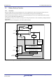
Table Of Contents
- Cover
- Notice
- General Precautions in the Handling of Microprocessing Unit and Microcontroller Unit Products
- How to Use This Manual
- Contents
- Features
- 1. Overview
- 2. CPU
- 2.1 Features
- 2.2 Register Set of the CPU
- 2.2.1 General-Purpose Registers (R0 to R15)
- 2.2.2 Control Registers
- 2.2.2.1 Interrupt Stack Pointer (ISP)/User Stack Pointer (USP)
- 2.2.2.2 Exception Table Register (EXTB)
- 2.2.2.3 Interrupt Table Register (INTB)
- 2.2.2.4 Program Counter (PC)
- 2.2.2.5 Processor Status Word (PSW)
- 2.2.2.6 Backup PC (BPC)
- 2.2.2.7 Backup PSW (BPSW)
- 2.2.2.8 Fast Interrupt Vector Register (FINTV)
- 2.2.2.9 Floating-Point Status Word (FPSW)
- 2.2.3 Accumulator
- 2.3 Processor Mode
- 2.4 Data Types
- 2.5 Endian
- 2.6 Vector Table
- 2.7 Operation of Instructions
- 2.8 Number of Cycles
- 3. Operating Modes
- 4. Address Space
- 5. I/O Registers
- 6. Resets
- 7. Option-Setting Memory (OFSM)
- 8. Voltage Detection Circuit (LVDAb)
- 9. Clock Generation Circuit
- 9.1 Overview
- 9.2 Register Descriptions
- 9.2.1 System Clock Control Register (SCKCR)
- 9.2.2 System Clock Control Register 3 (SCKCR3)
- 9.2.3 PLL Control Register (PLLCR)
- 9.2.4 PLL Control Register 2 (PLLCR2)
- 9.2.5 USB-dedicated PLL Control Register (UPLLCR)
- 9.2.6 USB-dedicated PLL Control Register 2 (UPLLCR2)
- 9.2.7 Main Clock Oscillator Control Register (MOSCCR)
- 9.2.8 Sub-Clock Oscillator Control Register (SOSCCR)
- 9.2.9 Low-Speed On-Chip Oscillator Control Register (LOCOCR)
- 9.2.10 IWDT-Dedicated On-Chip Oscillator Control Register (ILOCOCR)
- 9.2.11 High-Speed On-Chip Oscillator Control Register (HOCOCR)
- 9.2.12 High-Speed On-Chip Oscillator Control Register 2 (HOCOCR2)
- 9.2.13 Oscillation Stabilization Flag Register (OSCOVFSR)
- 9.2.14 Oscillation Stop Detection Control Register (OSTDCR)
- 9.2.15 Oscillation Stop Detection Status Register (OSTDSR)
- 9.2.16 Main Clock Oscillator Wait Control Register (MOSCWTCR)
- 9.2.17 CLKOUT Output Control Register (CKOCR)
- 9.2.18 Main Clock Oscillator Forced Oscillation Control Register (MOFCR)
- 9.2.19 Memory Wait Cycle Setting Register (MEMWAIT)
- 9.2.20 Low-Speed On-Chip Oscillator Trimming Register (LOCOTRR)
- 9.2.21 IWDT-Dedicated On-Chip Oscillator Trimming Register (ILOCOTRR)
- 9.2.22 High-Speed On-Chip Oscillator Trimming Register n (HOCOTRRn) (n = 0, 3)
- 9.3 Main Clock Oscillator
- 9.4 Sub-Clock Oscillator
- 9.5 Dedicated Clock Oscillator for Bluetooth
- 9.6 Oscillation Stop Detection Function
- 9.7 PLL Circuit
- 9.8 Internal Clock
- 9.9 Usage Notes
- 10. Clock Frequency Accuracy Measurement Circuit (CAC)
- 10.1 Overview
- 10.2 Register Descriptions
- 10.2.1 CAC Control Register 0 (CACR0)
- 10.2.2 CAC Control Register 1 (CACR1)
- 10.2.3 CAC Control Register 2 (CACR2)
- 10.2.4 CAC Interrupt Request Enable Register (CAICR)
- 10.2.5 CAC Status Register (CASTR)
- 10.2.6 CAC Upper-Limit Value Setting Register (CAULVR)
- 10.2.7 CAC Lower-Limit Value Setting Register (CALLVR)
- 10.2.8 CAC Counter Buffer Register (CACNTBR)
- 10.3 Operation
- 10.4 Interrupt Requests
- 10.5 Usage Notes
- 11. Low Power Consumption
- 11.1 Overview
- 11.2 Register Descriptions
- 11.2.1 Standby Control Register (SBYCR)
- 11.2.2 Module Stop Control Register A (MSTPCRA)
- 11.2.3 Module Stop Control Register B (MSTPCRB)
- 11.2.4 Module Stop Control Register C (MSTPCRC)
- 11.2.5 Module Stop Control Register D (MSTPCRD)
- 11.2.6 Operating Power Control Register (OPCCR)
- 11.2.7 Sub Operating Power Control Register (SOPCCR)
- 11.2.8 Sleep Mode Return Clock Source Switching Register (RSTCKCR)
- 11.3 Reducing Power Consumption by Switching Clock Signals
- 11.4 Module Stop Function
- 11.5 Function for Lower Operating Power Consumption
- 11.6 Low Power Consumption Modes
- 11.7 Usage Notes
- 12. Battery Backup Function
- 13. Register Write Protection Function
- 14. Exception Handling
- 15. Interrupt Controller (ICUb)
- 15.1 Overview
- 15.2 Register Descriptions
- 15.2.1 Interrupt Request Register n (IRn) (n = interrupt vector number)
- 15.2.2 Interrupt Request Enable Register m (IERm) (m = 02h to 1Fh)
- 15.2.3 Interrupt Source Priority Register n (IPRn) (n = interrupt vector number)
- 15.2.4 Fast Interrupt Set Register (FIR)
- 15.2.5 Software Interrupt Generation Register (SWINTR)
- 15.2.6 DTC Transfer Request Enable Register n (DTCERn) (n = interrupt vector number)
- 15.2.7 DMAC Trigger Select Register m (DMRSRm) (m = DMAC channel number)
- 15.2.8 IRQ Control Register i (IRQCRi) (i = 0, 1, and 4 to 7)
- 15.2.9 IRQ Pin Digital Filter Enable Register 0 (IRQFLTE0)
- 15.2.10 IRQ Pin Digital Filter Setting Register 0 (IRQFLTC0)
- 15.2.11 Non-Maskable Interrupt Status Register (NMISR)
- 15.2.12 Non-Maskable Interrupt Enable Register (NMIER)
- 15.2.13 Non-Maskable Interrupt Status Clear Register (NMICLR)
- 15.2.14 NMI Pin Interrupt Control Register (NMICR)
- 15.2.15 NMI Pin Digital Filter Enable Register (NMIFLTE)
- 15.2.16 NMI Pin Digital Filter Setting Register (NMIFLTC)
- 15.3 Vector Table
- 15.4 Interrupt Operation
- 15.5 Non-maskable Interrupt Operation
- 15.6 Return from Power-Down States
- 15.7 Usage Note
- 16. Buses
- 17. Memory-Protection Unit (MPU)
- 17.1 Overview
- 17.2 Register Descriptions
- 17.2.1 Region-n Start Page Number Register (RSPAGEn) (n = 0 to 7)
- 17.2.2 Region-n End Page Number Register (REPAGEn) (n = 0 to 7)
- 17.2.3 Memory-Protection Enable Register (MPEN)
- 17.2.4 Background Access Control Register (MPBAC)
- 17.2.5 Memory-Protection Error Status-Clearing Register (MPECLR)
- 17.2.6 Memory-Protection Error Status Register (MPESTS)
- 17.2.7 Data Memory-Protection Error Address Register (MPDEA)
- 17.2.8 Region Search Address Register (MPSA)
- 17.2.9 Region Search Operation Register (MPOPS)
- 17.2.10 Region Invalidation Operation Register (MPOPI)
- 17.2.11 Instruction-Hit Region Register (MHITI)
- 17.2.12 Data-Hit Region Register (MHITD)
- 17.3 Functions
- 17.4 Procedures for Using Memory Protection
- 18. DMA Controller (DMACA)
- 18.1 Overview
- 18.2 Register Descriptions
- 18.2.1 DMA Source Address Register (DMSAR)
- 18.2.2 DMA Destination Address Register (DMDAR)
- 18.2.3 DMA Transfer Count Register (DMCRA)
- 18.2.4 DMA Block Transfer Count Register (DMCRB)
- 18.2.5 DMA Transfer Mode Register (DMTMD)
- 18.2.6 DMA Interrupt Setting Register (DMINT)
- 18.2.7 DMA Address Mode Register (DMAMD)
- 18.2.8 DMA Offset Register (DMOFR)
- 18.2.9 DMA Transfer Enable Register (DMCNT)
- 18.2.10 DMA Software Start Register (DMREQ)
- 18.2.11 DMA Status Register (DMSTS)
- 18.2.12 DMA Activation Source Flag Control Register (DMCSL)
- 18.2.13 DMA Module Activation Register (DMAST)
- 18.3 Operation
- 18.4 Ending DMA Transfer
- 18.5 Interrupts
- 18.6 Event Link Function
- 18.7 Low Power Consumption Function
- 18.8 Usage Notes
- 18.8.1 DMA Transfer to Peripheral Modules
- 18.8.2 Access to the Registers during DMA Transfer
- 18.8.3 DMA Transfer to Reserved Areas
- 18.8.4 Interrupt Request by the DMA Activation Source Flag Control Register (DMCSL) at the End of each Transfer
- 18.8.5 Setting of DMAC Activation Source Select Register of the Interrupt Controller (ICU.DMRSRm)
- 18.8.6 Suspending or Restarting DMA Activation
- 19. Data Transfer Controller (DTCa)
- 19.1 Overview
- 19.2 Register Descriptions
- 19.2.1 DTC Mode Register A (MRA)
- 19.2.2 DTC Mode Register B (MRB)
- 19.2.3 DTC Transfer Source Register (SAR)
- 19.2.4 DTC Transfer Destination Register (DAR)
- 19.2.5 DTC Transfer Count Register A (CRA)
- 19.2.6 DTC Transfer Count Register B (CRB)
- 19.2.7 DTC Control Register (DTCCR)
- 19.2.8 DTC Vector Base Register (DTCVBR)
- 19.2.9 DTC Address Mode Register (DTCADMOD)
- 19.2.10 DTC Module Start Register (DTCST)
- 19.2.11 DTC Status Register (DTCSTS)
- 19.3 Request Sources
- 19.4 Operation

R01UH0823EJ0110 Rev.1.10 Page 253 of 1852
Nov 30, 2020
RX23W Group 11. Low Power Consumption
11.6.3 Software Standby Mode
11.6.3.1 Entry to Software Standby Mode
When a WAIT instruction is executed with the SBYCR.SSBY bit set to 1, a transition to software standby mode is made.
In this mode, the CPU, on-chip peripheral functions, and all the other functions except the sub-clock oscillator stop.
However, the contents of the CPU internal registers, RAM data, the states of on-chip peripheral functions, the I/O ports,
and the sub-clock oscillator are retained. Software standby mode allows significant reduction in power consumption
because the oscillator stops in this mode.
Set the DMAST.DMST bit of the DMAC and the DTCST.DTCST bit of the DTC to 0 before executing the WAIT
instruction.
When the WDT is used, the WDT stops counting when software standby mode is entered.
Counting by the IWDT stops if a transition to software standby mode is made while the IWDT is being used in auto-start
mode and the OFS0.IWDTSLCSTP bit is 1. In the same way, counting by the IWDT stops if a transition to software
standby mode is made while the IWDT is being used in register start mode and the IWDTCSTPR.SLCSTP bit is 1.
Furthermore, counting by the IWDT continues if a transition to software standby mode is made while the IWDT is being
used in auto-start mode and the OFS0.IWDTSLCSTP bit is 0 (counting by the IWDT continues through transitions to
low power consumption modes). In the same way, counting by the IWDT continues if a transition to software standby
mode is made while the IWDT is being used in register start mode and the IWDTCSTPR.SLCSTP bit is 0.
To use software standby mode, make the following settings and then execute a WAIT instruction.
(1) Set the PSW.I bit*
1
of the CPU to 0.
(2) Set the interrupt request destination*
2
to be used for recovery from software standby mode to the CPU.
(3) Set the priority*
3
of the interrupt to be used for recovery from software standby mode to a level higher than the
setting of the PSW.IPL[3:0] bits*
1
of the CPU.
(4) Set the IERm.IENj bit*
3
to 1 for the interrupt.
(5) Read the I/O register that is written last and confirm that the written value has been reflected.
(6) Execute a WAIT instruction (executing a WAIT instruction causes automatic setting of the PSW.I bit*
1
of the CPU
to 1).
Note 1. For details, refer to section 2, CPU.
Note 2. For details, refer to section 15.4.3, Selecting Interrupt Request Destinations.
Note 3. For details, refer to section 15, Interrupt Controller (ICUb).