
User's Manual
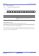
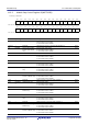

Table Of Contents
- Cover
- Notice
- General Precautions in the Handling of Microprocessing Unit and Microcontroller Unit Products
- How to Use This Manual
- Contents
- Features
- 1. Overview
- 2. CPU
- 2.1 Features
- 2.2 Register Set of the CPU
- 2.2.1 General-Purpose Registers (R0 to R15)
- 2.2.2 Control Registers
- 2.2.2.1 Interrupt Stack Pointer (ISP)/User Stack Pointer (USP)
- 2.2.2.2 Exception Table Register (EXTB)
- 2.2.2.3 Interrupt Table Register (INTB)
- 2.2.2.4 Program Counter (PC)
- 2.2.2.5 Processor Status Word (PSW)
- 2.2.2.6 Backup PC (BPC)
- 2.2.2.7 Backup PSW (BPSW)
- 2.2.2.8 Fast Interrupt Vector Register (FINTV)
- 2.2.2.9 Floating-Point Status Word (FPSW)
- 2.2.3 Accumulator
- 2.3 Processor Mode
- 2.4 Data Types
- 2.5 Endian
- 2.6 Vector Table
- 2.7 Operation of Instructions
- 2.8 Number of Cycles
- 3. Operating Modes
- 4. Address Space
- 5. I/O Registers
- 6. Resets
- 7. Option-Setting Memory (OFSM)
- 8. Voltage Detection Circuit (LVDAb)
- 9. Clock Generation Circuit
- 9.1 Overview
- 9.2 Register Descriptions
- 9.2.1 System Clock Control Register (SCKCR)
- 9.2.2 System Clock Control Register 3 (SCKCR3)
- 9.2.3 PLL Control Register (PLLCR)
- 9.2.4 PLL Control Register 2 (PLLCR2)
- 9.2.5 USB-dedicated PLL Control Register (UPLLCR)
- 9.2.6 USB-dedicated PLL Control Register 2 (UPLLCR2)
- 9.2.7 Main Clock Oscillator Control Register (MOSCCR)
- 9.2.8 Sub-Clock Oscillator Control Register (SOSCCR)
- 9.2.9 Low-Speed On-Chip Oscillator Control Register (LOCOCR)
- 9.2.10 IWDT-Dedicated On-Chip Oscillator Control Register (ILOCOCR)
- 9.2.11 High-Speed On-Chip Oscillator Control Register (HOCOCR)
- 9.2.12 High-Speed On-Chip Oscillator Control Register 2 (HOCOCR2)
- 9.2.13 Oscillation Stabilization Flag Register (OSCOVFSR)
- 9.2.14 Oscillation Stop Detection Control Register (OSTDCR)
- 9.2.15 Oscillation Stop Detection Status Register (OSTDSR)
- 9.2.16 Main Clock Oscillator Wait Control Register (MOSCWTCR)
- 9.2.17 CLKOUT Output Control Register (CKOCR)
- 9.2.18 Main Clock Oscillator Forced Oscillation Control Register (MOFCR)
- 9.2.19 Memory Wait Cycle Setting Register (MEMWAIT)
- 9.2.20 Low-Speed On-Chip Oscillator Trimming Register (LOCOTRR)
- 9.2.21 IWDT-Dedicated On-Chip Oscillator Trimming Register (ILOCOTRR)
- 9.2.22 High-Speed On-Chip Oscillator Trimming Register n (HOCOTRRn) (n = 0, 3)
- 9.3 Main Clock Oscillator
- 9.4 Sub-Clock Oscillator
- 9.5 Dedicated Clock Oscillator for Bluetooth
- 9.6 Oscillation Stop Detection Function
- 9.7 PLL Circuit
- 9.8 Internal Clock
- 9.9 Usage Notes
- 10. Clock Frequency Accuracy Measurement Circuit (CAC)
- 10.1 Overview
- 10.2 Register Descriptions
- 10.2.1 CAC Control Register 0 (CACR0)
- 10.2.2 CAC Control Register 1 (CACR1)
- 10.2.3 CAC Control Register 2 (CACR2)
- 10.2.4 CAC Interrupt Request Enable Register (CAICR)
- 10.2.5 CAC Status Register (CASTR)
- 10.2.6 CAC Upper-Limit Value Setting Register (CAULVR)
- 10.2.7 CAC Lower-Limit Value Setting Register (CALLVR)
- 10.2.8 CAC Counter Buffer Register (CACNTBR)
- 10.3 Operation
- 10.4 Interrupt Requests
- 10.5 Usage Notes
- 11. Low Power Consumption
- 11.1 Overview
- 11.2 Register Descriptions
- 11.2.1 Standby Control Register (SBYCR)
- 11.2.2 Module Stop Control Register A (MSTPCRA)
- 11.2.3 Module Stop Control Register B (MSTPCRB)
- 11.2.4 Module Stop Control Register C (MSTPCRC)
- 11.2.5 Module Stop Control Register D (MSTPCRD)
- 11.2.6 Operating Power Control Register (OPCCR)
- 11.2.7 Sub Operating Power Control Register (SOPCCR)
- 11.2.8 Sleep Mode Return Clock Source Switching Register (RSTCKCR)
- 11.3 Reducing Power Consumption by Switching Clock Signals
- 11.4 Module Stop Function
- 11.5 Function for Lower Operating Power Consumption
- 11.6 Low Power Consumption Modes
- 11.7 Usage Notes
- 12. Battery Backup Function
- 13. Register Write Protection Function
- 14. Exception Handling
- 15. Interrupt Controller (ICUb)
- 15.1 Overview
- 15.2 Register Descriptions
- 15.2.1 Interrupt Request Register n (IRn) (n = interrupt vector number)
- 15.2.2 Interrupt Request Enable Register m (IERm) (m = 02h to 1Fh)
- 15.2.3 Interrupt Source Priority Register n (IPRn) (n = interrupt vector number)
- 15.2.4 Fast Interrupt Set Register (FIR)
- 15.2.5 Software Interrupt Generation Register (SWINTR)
- 15.2.6 DTC Transfer Request Enable Register n (DTCERn) (n = interrupt vector number)
- 15.2.7 DMAC Trigger Select Register m (DMRSRm) (m = DMAC channel number)
- 15.2.8 IRQ Control Register i (IRQCRi) (i = 0, 1, and 4 to 7)
- 15.2.9 IRQ Pin Digital Filter Enable Register 0 (IRQFLTE0)
- 15.2.10 IRQ Pin Digital Filter Setting Register 0 (IRQFLTC0)
- 15.2.11 Non-Maskable Interrupt Status Register (NMISR)
- 15.2.12 Non-Maskable Interrupt Enable Register (NMIER)
- 15.2.13 Non-Maskable Interrupt Status Clear Register (NMICLR)
- 15.2.14 NMI Pin Interrupt Control Register (NMICR)
- 15.2.15 NMI Pin Digital Filter Enable Register (NMIFLTE)
- 15.2.16 NMI Pin Digital Filter Setting Register (NMIFLTC)
- 15.3 Vector Table
- 15.4 Interrupt Operation
- 15.5 Non-maskable Interrupt Operation
- 15.6 Return from Power-Down States
- 15.7 Usage Note
- 16. Buses
- 17. Memory-Protection Unit (MPU)
- 17.1 Overview
- 17.2 Register Descriptions
- 17.2.1 Region-n Start Page Number Register (RSPAGEn) (n = 0 to 7)
- 17.2.2 Region-n End Page Number Register (REPAGEn) (n = 0 to 7)
- 17.2.3 Memory-Protection Enable Register (MPEN)
- 17.2.4 Background Access Control Register (MPBAC)
- 17.2.5 Memory-Protection Error Status-Clearing Register (MPECLR)
- 17.2.6 Memory-Protection Error Status Register (MPESTS)
- 17.2.7 Data Memory-Protection Error Address Register (MPDEA)
- 17.2.8 Region Search Address Register (MPSA)
- 17.2.9 Region Search Operation Register (MPOPS)
- 17.2.10 Region Invalidation Operation Register (MPOPI)
- 17.2.11 Instruction-Hit Region Register (MHITI)
- 17.2.12 Data-Hit Region Register (MHITD)
- 17.3 Functions
- 17.4 Procedures for Using Memory Protection
- 18. DMA Controller (DMACA)
- 18.1 Overview
- 18.2 Register Descriptions
- 18.2.1 DMA Source Address Register (DMSAR)
- 18.2.2 DMA Destination Address Register (DMDAR)
- 18.2.3 DMA Transfer Count Register (DMCRA)
- 18.2.4 DMA Block Transfer Count Register (DMCRB)
- 18.2.5 DMA Transfer Mode Register (DMTMD)
- 18.2.6 DMA Interrupt Setting Register (DMINT)
- 18.2.7 DMA Address Mode Register (DMAMD)
- 18.2.8 DMA Offset Register (DMOFR)
- 18.2.9 DMA Transfer Enable Register (DMCNT)
- 18.2.10 DMA Software Start Register (DMREQ)
- 18.2.11 DMA Status Register (DMSTS)
- 18.2.12 DMA Activation Source Flag Control Register (DMCSL)
- 18.2.13 DMA Module Activation Register (DMAST)
- 18.3 Operation
- 18.4 Ending DMA Transfer
- 18.5 Interrupts
- 18.6 Event Link Function
- 18.7 Low Power Consumption Function
- 18.8 Usage Notes
- 18.8.1 DMA Transfer to Peripheral Modules
- 18.8.2 Access to the Registers during DMA Transfer
- 18.8.3 DMA Transfer to Reserved Areas
- 18.8.4 Interrupt Request by the DMA Activation Source Flag Control Register (DMCSL) at the End of each Transfer
- 18.8.5 Setting of DMAC Activation Source Select Register of the Interrupt Controller (ICU.DMRSRm)
- 18.8.6 Suspending or Restarting DMA Activation
- 19. Data Transfer Controller (DTCa)
- 19.1 Overview
- 19.2 Register Descriptions
- 19.2.1 DTC Mode Register A (MRA)
- 19.2.2 DTC Mode Register B (MRB)
- 19.2.3 DTC Transfer Source Register (SAR)
- 19.2.4 DTC Transfer Destination Register (DAR)
- 19.2.5 DTC Transfer Count Register A (CRA)
- 19.2.6 DTC Transfer Count Register B (CRB)
- 19.2.7 DTC Control Register (DTCCR)
- 19.2.8 DTC Vector Base Register (DTCVBR)
- 19.2.9 DTC Address Mode Register (DTCADMOD)
- 19.2.10 DTC Module Start Register (DTCST)
- 19.2.11 DTC Status Register (DTCSTS)
- 19.3 Request Sources
- 19.4 Operation

R01UH0823EJ0110 Rev.1.10 Page 239 of 1852
Nov 30, 2020
RX23W Group 11. Low Power Consumption
11.2.6 Operating Power Control Register (OPCCR)
Note: Set the PRCR.PRC1 bit to 1 (write enabled) before rewriting this register.
The OPCCR register is used to reduce power consumption in normal operating mode, sleep mode, and deep sleep mode.
Power consumption can be reduced according to the operating frequency and operating voltage to be used by the OPCCR
setting.
The OPCCR register cannot be rewritten under the following conditions:
• When the OPCCR.OPCMTSF flag is 1 (during transition)
• Time period from WAIT instruction execution for a sleep mode transition, until exit from sleep mode to normal
operation
• Time period from WAIT instruction execution for a deep sleep mode transition, until exit from deep sleep mode to
normal operation
• When the SOPCCR.SOPCM bit is 1 (low-speed operating mode)
The OPCCR register cannot be rewritten while the flash memory is being programmed or erased (P/E).
For the procedures of changing operating power control modes, refer to Function in section 11.5, Function for Lower
Operating Power Consumption.
During sleep mode or mode transitions, do not write to the registers related to system control (indicated by ‘SYSTEM’ in
the Module Symbol column in Table 5.1, List of I/O Registers (Address Order)).
OPCM[2:0] Bits (Operating Power Control Mode Select)
The OPCM[2:0] bits select operating power control mode in normal operating mode, sleep mode, and deep sleep mode.
Table 11.4 shows the relationship between operating power control modes, the OPCM[2:0] and SOPCM bit settings,
and the operating frequency and voltage ranges.
OPCMTSF Flag (Operating Power Control Mode Transition Status Flag)
This flag indicates the switching control state during and after operating power mode transition.
This flag becomes 1 when the value of the OPCM[2:0] bits is rewritten, and 0 when mode transition is completed. Read
this flag and confirm that it is 0 before proceeding to the next processing. Only rewrite the OPCM[2:0] bits when this
flag is 0.
Address(es): 0008 00A0h
b7 b6 b5 b4 b3 b2 b1 b0
———
OPCM
TSF
— OPCM[2:0]
Value after reset:
00000010
Bit Symbol Bit Name Description R/W
b2 to b0 OPCM[2:0] Operating Power Control
Mode Select
b2 b0
0 0 0: High-speed operating mode
0 1 0: Middle-speed operating mode
Settings other than above are prohibited.
R/W
b3 — Reserved This bit is read as 0. The write value should be 0. R/W
b4 OPCMTSF Operating Power Control
Mode Transition Status
Flag
0: Transition completed
1: During transition
R
b7 to b5 — Reserved These bits are read as 0. The write value should be 0. R/W