
User's Manual
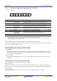
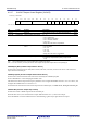
Table Of Contents
- Cover
- Notice
- General Precautions in the Handling of Microprocessing Unit and Microcontroller Unit Products
- How to Use This Manual
- Contents
- Features
- 1. Overview
- 2. CPU
- 2.1 Features
- 2.2 Register Set of the CPU
- 2.2.1 General-Purpose Registers (R0 to R15)
- 2.2.2 Control Registers
- 2.2.2.1 Interrupt Stack Pointer (ISP)/User Stack Pointer (USP)
- 2.2.2.2 Exception Table Register (EXTB)
- 2.2.2.3 Interrupt Table Register (INTB)
- 2.2.2.4 Program Counter (PC)
- 2.2.2.5 Processor Status Word (PSW)
- 2.2.2.6 Backup PC (BPC)
- 2.2.2.7 Backup PSW (BPSW)
- 2.2.2.8 Fast Interrupt Vector Register (FINTV)
- 2.2.2.9 Floating-Point Status Word (FPSW)
- 2.2.3 Accumulator
- 2.3 Processor Mode
- 2.4 Data Types
- 2.5 Endian
- 2.6 Vector Table
- 2.7 Operation of Instructions
- 2.8 Number of Cycles
- 3. Operating Modes
- 4. Address Space
- 5. I/O Registers
- 6. Resets
- 7. Option-Setting Memory (OFSM)
- 8. Voltage Detection Circuit (LVDAb)
- 9. Clock Generation Circuit
- 9.1 Overview
- 9.2 Register Descriptions
- 9.2.1 System Clock Control Register (SCKCR)
- 9.2.2 System Clock Control Register 3 (SCKCR3)
- 9.2.3 PLL Control Register (PLLCR)
- 9.2.4 PLL Control Register 2 (PLLCR2)
- 9.2.5 USB-dedicated PLL Control Register (UPLLCR)
- 9.2.6 USB-dedicated PLL Control Register 2 (UPLLCR2)
- 9.2.7 Main Clock Oscillator Control Register (MOSCCR)
- 9.2.8 Sub-Clock Oscillator Control Register (SOSCCR)
- 9.2.9 Low-Speed On-Chip Oscillator Control Register (LOCOCR)
- 9.2.10 IWDT-Dedicated On-Chip Oscillator Control Register (ILOCOCR)
- 9.2.11 High-Speed On-Chip Oscillator Control Register (HOCOCR)
- 9.2.12 High-Speed On-Chip Oscillator Control Register 2 (HOCOCR2)
- 9.2.13 Oscillation Stabilization Flag Register (OSCOVFSR)
- 9.2.14 Oscillation Stop Detection Control Register (OSTDCR)
- 9.2.15 Oscillation Stop Detection Status Register (OSTDSR)
- 9.2.16 Main Clock Oscillator Wait Control Register (MOSCWTCR)
- 9.2.17 CLKOUT Output Control Register (CKOCR)
- 9.2.18 Main Clock Oscillator Forced Oscillation Control Register (MOFCR)
- 9.2.19 Memory Wait Cycle Setting Register (MEMWAIT)
- 9.2.20 Low-Speed On-Chip Oscillator Trimming Register (LOCOTRR)
- 9.2.21 IWDT-Dedicated On-Chip Oscillator Trimming Register (ILOCOTRR)
- 9.2.22 High-Speed On-Chip Oscillator Trimming Register n (HOCOTRRn) (n = 0, 3)
- 9.3 Main Clock Oscillator
- 9.4 Sub-Clock Oscillator
- 9.5 Dedicated Clock Oscillator for Bluetooth
- 9.6 Oscillation Stop Detection Function
- 9.7 PLL Circuit
- 9.8 Internal Clock
- 9.9 Usage Notes
- 10. Clock Frequency Accuracy Measurement Circuit (CAC)
- 10.1 Overview
- 10.2 Register Descriptions
- 10.2.1 CAC Control Register 0 (CACR0)
- 10.2.2 CAC Control Register 1 (CACR1)
- 10.2.3 CAC Control Register 2 (CACR2)
- 10.2.4 CAC Interrupt Request Enable Register (CAICR)
- 10.2.5 CAC Status Register (CASTR)
- 10.2.6 CAC Upper-Limit Value Setting Register (CAULVR)
- 10.2.7 CAC Lower-Limit Value Setting Register (CALLVR)
- 10.2.8 CAC Counter Buffer Register (CACNTBR)
- 10.3 Operation
- 10.4 Interrupt Requests
- 10.5 Usage Notes
- 11. Low Power Consumption
- 11.1 Overview
- 11.2 Register Descriptions
- 11.2.1 Standby Control Register (SBYCR)
- 11.2.2 Module Stop Control Register A (MSTPCRA)
- 11.2.3 Module Stop Control Register B (MSTPCRB)
- 11.2.4 Module Stop Control Register C (MSTPCRC)
- 11.2.5 Module Stop Control Register D (MSTPCRD)
- 11.2.6 Operating Power Control Register (OPCCR)
- 11.2.7 Sub Operating Power Control Register (SOPCCR)
- 11.2.8 Sleep Mode Return Clock Source Switching Register (RSTCKCR)
- 11.3 Reducing Power Consumption by Switching Clock Signals
- 11.4 Module Stop Function
- 11.5 Function for Lower Operating Power Consumption
- 11.6 Low Power Consumption Modes
- 11.7 Usage Notes
- 12. Battery Backup Function
- 13. Register Write Protection Function
- 14. Exception Handling
- 15. Interrupt Controller (ICUb)
- 15.1 Overview
- 15.2 Register Descriptions
- 15.2.1 Interrupt Request Register n (IRn) (n = interrupt vector number)
- 15.2.2 Interrupt Request Enable Register m (IERm) (m = 02h to 1Fh)
- 15.2.3 Interrupt Source Priority Register n (IPRn) (n = interrupt vector number)
- 15.2.4 Fast Interrupt Set Register (FIR)
- 15.2.5 Software Interrupt Generation Register (SWINTR)
- 15.2.6 DTC Transfer Request Enable Register n (DTCERn) (n = interrupt vector number)
- 15.2.7 DMAC Trigger Select Register m (DMRSRm) (m = DMAC channel number)
- 15.2.8 IRQ Control Register i (IRQCRi) (i = 0, 1, and 4 to 7)
- 15.2.9 IRQ Pin Digital Filter Enable Register 0 (IRQFLTE0)
- 15.2.10 IRQ Pin Digital Filter Setting Register 0 (IRQFLTC0)
- 15.2.11 Non-Maskable Interrupt Status Register (NMISR)
- 15.2.12 Non-Maskable Interrupt Enable Register (NMIER)
- 15.2.13 Non-Maskable Interrupt Status Clear Register (NMICLR)
- 15.2.14 NMI Pin Interrupt Control Register (NMICR)
- 15.2.15 NMI Pin Digital Filter Enable Register (NMIFLTE)
- 15.2.16 NMI Pin Digital Filter Setting Register (NMIFLTC)
- 15.3 Vector Table
- 15.4 Interrupt Operation
- 15.5 Non-maskable Interrupt Operation
- 15.6 Return from Power-Down States
- 15.7 Usage Note
- 16. Buses
- 17. Memory-Protection Unit (MPU)
- 17.1 Overview
- 17.2 Register Descriptions
- 17.2.1 Region-n Start Page Number Register (RSPAGEn) (n = 0 to 7)
- 17.2.2 Region-n End Page Number Register (REPAGEn) (n = 0 to 7)
- 17.2.3 Memory-Protection Enable Register (MPEN)
- 17.2.4 Background Access Control Register (MPBAC)
- 17.2.5 Memory-Protection Error Status-Clearing Register (MPECLR)
- 17.2.6 Memory-Protection Error Status Register (MPESTS)
- 17.2.7 Data Memory-Protection Error Address Register (MPDEA)
- 17.2.8 Region Search Address Register (MPSA)
- 17.2.9 Region Search Operation Register (MPOPS)
- 17.2.10 Region Invalidation Operation Register (MPOPI)
- 17.2.11 Instruction-Hit Region Register (MHITI)
- 17.2.12 Data-Hit Region Register (MHITD)
- 17.3 Functions
- 17.4 Procedures for Using Memory Protection
- 18. DMA Controller (DMACA)
- 18.1 Overview
- 18.2 Register Descriptions
- 18.2.1 DMA Source Address Register (DMSAR)
- 18.2.2 DMA Destination Address Register (DMDAR)
- 18.2.3 DMA Transfer Count Register (DMCRA)
- 18.2.4 DMA Block Transfer Count Register (DMCRB)
- 18.2.5 DMA Transfer Mode Register (DMTMD)
- 18.2.6 DMA Interrupt Setting Register (DMINT)
- 18.2.7 DMA Address Mode Register (DMAMD)
- 18.2.8 DMA Offset Register (DMOFR)
- 18.2.9 DMA Transfer Enable Register (DMCNT)
- 18.2.10 DMA Software Start Register (DMREQ)
- 18.2.11 DMA Status Register (DMSTS)
- 18.2.12 DMA Activation Source Flag Control Register (DMCSL)
- 18.2.13 DMA Module Activation Register (DMAST)
- 18.3 Operation
- 18.4 Ending DMA Transfer
- 18.5 Interrupts
- 18.6 Event Link Function
- 18.7 Low Power Consumption Function
- 18.8 Usage Notes
- 18.8.1 DMA Transfer to Peripheral Modules
- 18.8.2 Access to the Registers during DMA Transfer
- 18.8.3 DMA Transfer to Reserved Areas
- 18.8.4 Interrupt Request by the DMA Activation Source Flag Control Register (DMCSL) at the End of each Transfer
- 18.8.5 Setting of DMAC Activation Source Select Register of the Interrupt Controller (ICU.DMRSRm)
- 18.8.6 Suspending or Restarting DMA Activation
- 19. Data Transfer Controller (DTCa)
- 19.1 Overview
- 19.2 Register Descriptions
- 19.2.1 DTC Mode Register A (MRA)
- 19.2.2 DTC Mode Register B (MRB)
- 19.2.3 DTC Transfer Source Register (SAR)
- 19.2.4 DTC Transfer Destination Register (DAR)
- 19.2.5 DTC Transfer Count Register A (CRA)
- 19.2.6 DTC Transfer Count Register B (CRB)
- 19.2.7 DTC Control Register (DTCCR)
- 19.2.8 DTC Vector Base Register (DTCVBR)
- 19.2.9 DTC Address Mode Register (DTCADMOD)
- 19.2.10 DTC Module Start Register (DTCST)
- 19.2.11 DTC Status Register (DTCSTS)
- 19.3 Request Sources
- 19.4 Operation

R01UH0823EJ0110 Rev.1.10 Page 193 of 1852
Nov 30, 2020
RX23W Group 9. Clock Generation Circuit
9.2.14 Oscillation Stop Detection Control Register (OSTDCR)
Note: Set the PRCR.PRC0 bit to 1 (write enabled) before rewriting this register.
OSTDIE Bit (Oscillation Stop Detection Interrupt Enable)
If the oscillation stop detection flag in the oscillation stop detection status register (OSTDSR.OSTDF) requires clearing,
do this after setting the OSTDIE bit to 0. Wait for at least two cycles of PCLKB before again setting the OSTDIE bit to 1.
According to the number of cycles for access to read a given I/O register, wait time longer than two cycles of PCLKB
may have to be secured.
OSTDE Bit (Oscillation Stop Detection Function Enable)
This bit enables or disables the oscillation stop detection function.
When the OSTDE bit is 1 (oscillation stop detection function enabled), the LOCO stop bit (LOCOCR.LCSTP) is set to 0
and the LOCO operation is started. The LOCO cannot be stopped while the oscillation stop detection function is enabled;
writing 1 (LOCO is stopped) to the LOCOCR.LCSTP bit is invalid.
When the oscillation stop detection flag in the oscillation stop detection status register (OSTDSR.OSTDF) is 1 (main
clock oscillation stop has been detected), writing 0 to the OSTDE bit is invalid.
When the OSTDE bit is 1, a transition cannot be made to software standby mode. To make a transition to software
standby mode, execute the WAIT instruction with the OSTDE bit being 0.
Address(es): 0008 0040h
b7 b6 b5 b4 b3 b2 b1 b0
OSTDE——————
OSTDI
E
Value after reset:
00000000
Bit Symbol Bit Name Description R/W
b0 OSTDIE Oscillation Stop Detection
Interrupt Enable
0: The oscillation stop detection interrupt is disabled. Oscillation stop
detection is not notified to the POE.
1: The oscillation stop detection interrupt is enabled. Oscillation stop
detection is notified to the POE.
R/W
b6 to b1 — Reserved These bits are read as 0. The write value should be 0. R/W
b7 OSTDE Oscillation Stop Detection
Function Enable
0: Oscillation stop detection function is disabled.
1: Oscillation stop detection function is enabled.
R/W