
User's Manual
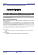
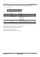
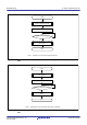
Table Of Contents
- Cover
- Notice
- General Precautions in the Handling of Microprocessing Unit and Microcontroller Unit Products
- How to Use This Manual
- Contents
- Features
- 1. Overview
- 2. CPU
- 2.1 Features
- 2.2 Register Set of the CPU
- 2.2.1 General-Purpose Registers (R0 to R15)
- 2.2.2 Control Registers
- 2.2.2.1 Interrupt Stack Pointer (ISP)/User Stack Pointer (USP)
- 2.2.2.2 Exception Table Register (EXTB)
- 2.2.2.3 Interrupt Table Register (INTB)
- 2.2.2.4 Program Counter (PC)
- 2.2.2.5 Processor Status Word (PSW)
- 2.2.2.6 Backup PC (BPC)
- 2.2.2.7 Backup PSW (BPSW)
- 2.2.2.8 Fast Interrupt Vector Register (FINTV)
- 2.2.2.9 Floating-Point Status Word (FPSW)
- 2.2.3 Accumulator
- 2.3 Processor Mode
- 2.4 Data Types
- 2.5 Endian
- 2.6 Vector Table
- 2.7 Operation of Instructions
- 2.8 Number of Cycles
- 3. Operating Modes
- 4. Address Space
- 5. I/O Registers
- 6. Resets
- 7. Option-Setting Memory (OFSM)
- 8. Voltage Detection Circuit (LVDAb)
- 9. Clock Generation Circuit
- 9.1 Overview
- 9.2 Register Descriptions
- 9.2.1 System Clock Control Register (SCKCR)
- 9.2.2 System Clock Control Register 3 (SCKCR3)
- 9.2.3 PLL Control Register (PLLCR)
- 9.2.4 PLL Control Register 2 (PLLCR2)
- 9.2.5 USB-dedicated PLL Control Register (UPLLCR)
- 9.2.6 USB-dedicated PLL Control Register 2 (UPLLCR2)
- 9.2.7 Main Clock Oscillator Control Register (MOSCCR)
- 9.2.8 Sub-Clock Oscillator Control Register (SOSCCR)
- 9.2.9 Low-Speed On-Chip Oscillator Control Register (LOCOCR)
- 9.2.10 IWDT-Dedicated On-Chip Oscillator Control Register (ILOCOCR)
- 9.2.11 High-Speed On-Chip Oscillator Control Register (HOCOCR)
- 9.2.12 High-Speed On-Chip Oscillator Control Register 2 (HOCOCR2)
- 9.2.13 Oscillation Stabilization Flag Register (OSCOVFSR)
- 9.2.14 Oscillation Stop Detection Control Register (OSTDCR)
- 9.2.15 Oscillation Stop Detection Status Register (OSTDSR)
- 9.2.16 Main Clock Oscillator Wait Control Register (MOSCWTCR)
- 9.2.17 CLKOUT Output Control Register (CKOCR)
- 9.2.18 Main Clock Oscillator Forced Oscillation Control Register (MOFCR)
- 9.2.19 Memory Wait Cycle Setting Register (MEMWAIT)
- 9.2.20 Low-Speed On-Chip Oscillator Trimming Register (LOCOTRR)
- 9.2.21 IWDT-Dedicated On-Chip Oscillator Trimming Register (ILOCOTRR)
- 9.2.22 High-Speed On-Chip Oscillator Trimming Register n (HOCOTRRn) (n = 0, 3)
- 9.3 Main Clock Oscillator
- 9.4 Sub-Clock Oscillator
- 9.5 Dedicated Clock Oscillator for Bluetooth
- 9.6 Oscillation Stop Detection Function
- 9.7 PLL Circuit
- 9.8 Internal Clock
- 9.9 Usage Notes
- 10. Clock Frequency Accuracy Measurement Circuit (CAC)
- 10.1 Overview
- 10.2 Register Descriptions
- 10.2.1 CAC Control Register 0 (CACR0)
- 10.2.2 CAC Control Register 1 (CACR1)
- 10.2.3 CAC Control Register 2 (CACR2)
- 10.2.4 CAC Interrupt Request Enable Register (CAICR)
- 10.2.5 CAC Status Register (CASTR)
- 10.2.6 CAC Upper-Limit Value Setting Register (CAULVR)
- 10.2.7 CAC Lower-Limit Value Setting Register (CALLVR)
- 10.2.8 CAC Counter Buffer Register (CACNTBR)
- 10.3 Operation
- 10.4 Interrupt Requests
- 10.5 Usage Notes
- 11. Low Power Consumption
- 11.1 Overview
- 11.2 Register Descriptions
- 11.2.1 Standby Control Register (SBYCR)
- 11.2.2 Module Stop Control Register A (MSTPCRA)
- 11.2.3 Module Stop Control Register B (MSTPCRB)
- 11.2.4 Module Stop Control Register C (MSTPCRC)
- 11.2.5 Module Stop Control Register D (MSTPCRD)
- 11.2.6 Operating Power Control Register (OPCCR)
- 11.2.7 Sub Operating Power Control Register (SOPCCR)
- 11.2.8 Sleep Mode Return Clock Source Switching Register (RSTCKCR)
- 11.3 Reducing Power Consumption by Switching Clock Signals
- 11.4 Module Stop Function
- 11.5 Function for Lower Operating Power Consumption
- 11.6 Low Power Consumption Modes
- 11.7 Usage Notes
- 12. Battery Backup Function
- 13. Register Write Protection Function
- 14. Exception Handling
- 15. Interrupt Controller (ICUb)
- 15.1 Overview
- 15.2 Register Descriptions
- 15.2.1 Interrupt Request Register n (IRn) (n = interrupt vector number)
- 15.2.2 Interrupt Request Enable Register m (IERm) (m = 02h to 1Fh)
- 15.2.3 Interrupt Source Priority Register n (IPRn) (n = interrupt vector number)
- 15.2.4 Fast Interrupt Set Register (FIR)
- 15.2.5 Software Interrupt Generation Register (SWINTR)
- 15.2.6 DTC Transfer Request Enable Register n (DTCERn) (n = interrupt vector number)
- 15.2.7 DMAC Trigger Select Register m (DMRSRm) (m = DMAC channel number)
- 15.2.8 IRQ Control Register i (IRQCRi) (i = 0, 1, and 4 to 7)
- 15.2.9 IRQ Pin Digital Filter Enable Register 0 (IRQFLTE0)
- 15.2.10 IRQ Pin Digital Filter Setting Register 0 (IRQFLTC0)
- 15.2.11 Non-Maskable Interrupt Status Register (NMISR)
- 15.2.12 Non-Maskable Interrupt Enable Register (NMIER)
- 15.2.13 Non-Maskable Interrupt Status Clear Register (NMICLR)
- 15.2.14 NMI Pin Interrupt Control Register (NMICR)
- 15.2.15 NMI Pin Digital Filter Enable Register (NMIFLTE)
- 15.2.16 NMI Pin Digital Filter Setting Register (NMIFLTC)
- 15.3 Vector Table
- 15.4 Interrupt Operation
- 15.5 Non-maskable Interrupt Operation
- 15.6 Return from Power-Down States
- 15.7 Usage Note
- 16. Buses
- 17. Memory-Protection Unit (MPU)
- 17.1 Overview
- 17.2 Register Descriptions
- 17.2.1 Region-n Start Page Number Register (RSPAGEn) (n = 0 to 7)
- 17.2.2 Region-n End Page Number Register (REPAGEn) (n = 0 to 7)
- 17.2.3 Memory-Protection Enable Register (MPEN)
- 17.2.4 Background Access Control Register (MPBAC)
- 17.2.5 Memory-Protection Error Status-Clearing Register (MPECLR)
- 17.2.6 Memory-Protection Error Status Register (MPESTS)
- 17.2.7 Data Memory-Protection Error Address Register (MPDEA)
- 17.2.8 Region Search Address Register (MPSA)
- 17.2.9 Region Search Operation Register (MPOPS)
- 17.2.10 Region Invalidation Operation Register (MPOPI)
- 17.2.11 Instruction-Hit Region Register (MHITI)
- 17.2.12 Data-Hit Region Register (MHITD)
- 17.3 Functions
- 17.4 Procedures for Using Memory Protection
- 18. DMA Controller (DMACA)
- 18.1 Overview
- 18.2 Register Descriptions
- 18.2.1 DMA Source Address Register (DMSAR)
- 18.2.2 DMA Destination Address Register (DMDAR)
- 18.2.3 DMA Transfer Count Register (DMCRA)
- 18.2.4 DMA Block Transfer Count Register (DMCRB)
- 18.2.5 DMA Transfer Mode Register (DMTMD)
- 18.2.6 DMA Interrupt Setting Register (DMINT)
- 18.2.7 DMA Address Mode Register (DMAMD)
- 18.2.8 DMA Offset Register (DMOFR)
- 18.2.9 DMA Transfer Enable Register (DMCNT)
- 18.2.10 DMA Software Start Register (DMREQ)
- 18.2.11 DMA Status Register (DMSTS)
- 18.2.12 DMA Activation Source Flag Control Register (DMCSL)
- 18.2.13 DMA Module Activation Register (DMAST)
- 18.3 Operation
- 18.4 Ending DMA Transfer
- 18.5 Interrupts
- 18.6 Event Link Function
- 18.7 Low Power Consumption Function
- 18.8 Usage Notes
- 18.8.1 DMA Transfer to Peripheral Modules
- 18.8.2 Access to the Registers during DMA Transfer
- 18.8.3 DMA Transfer to Reserved Areas
- 18.8.4 Interrupt Request by the DMA Activation Source Flag Control Register (DMCSL) at the End of each Transfer
- 18.8.5 Setting of DMAC Activation Source Select Register of the Interrupt Controller (ICU.DMRSRm)
- 18.8.6 Suspending or Restarting DMA Activation
- 19. Data Transfer Controller (DTCa)
- 19.1 Overview
- 19.2 Register Descriptions
- 19.2.1 DTC Mode Register A (MRA)
- 19.2.2 DTC Mode Register B (MRB)
- 19.2.3 DTC Transfer Source Register (SAR)
- 19.2.4 DTC Transfer Destination Register (DAR)
- 19.2.5 DTC Transfer Count Register A (CRA)
- 19.2.6 DTC Transfer Count Register B (CRB)
- 19.2.7 DTC Control Register (DTCCR)
- 19.2.8 DTC Vector Base Register (DTCVBR)
- 19.2.9 DTC Address Mode Register (DTCADMOD)
- 19.2.10 DTC Module Start Register (DTCST)
- 19.2.11 DTC Status Register (DTCSTS)
- 19.3 Request Sources
- 19.4 Operation

R01UH0823EJ0110 Rev.1.10 Page 191 of 1852
Nov 30, 2020
RX23W Group 9. Clock Generation Circuit
9.2.13 Oscillation Stabilization Flag Register (OSCOVFSR)
Note 1. The HCOVF value after a reset is 1 when the HOCO oscillation enable bit in option function selection register 1
(OFS1.HOCOEN) is 0. The HCOVF value after a reset is 0 when the OFS1.HOCOEN bit is 1.
Note 2. When an appropriate value is set in the wait control register for each oscillator. If a set value (wait time) is not adequate, clock
supply starts before oscillation becomes stable.
The OSCOVFSR register monitors whether oscillation of each oscillator has become stable.
If a wait control register is provided for each oscillator, specify a wait time that is longer than or equal to the stabilization
time of the corresponding oscillation circuit.
MOOVF Flag (Main Clock Oscillation Stabilization Flag)
This flag indicates whether oscillation of the main clock is stable.
[Setting condition]
• After the MOSCCR.MOSTP bit is set to 0 (main clock oscillator is operating) when the MOSTP bit is 1 (main clock
oscillator is stopped), the corresponding time set in the MOSCWTCR register has elapsed and supply of the main
clock is started to the MCU internally.
[Clearing condition]
• After the MOSCCR.MOSTP bit is set to 1, the processing to stop the oscillation of the main clock oscillator is
completed.
PLOVF Flag (PLL Clock Oscillation Stabilization Flag)
This flag indicates whether oscillation of the PLL clock is stable.
[Setting condition]
After the PLLCR2.PLLEN is set to 0 (PLL is operating) when the PLLEN bit is 1 (PLL is stopped), the MOOVF flag
becomes 1, the PLL clock oscillation stabilization time (tPLL) has elapsed, and supply of the PLL clock is started to the
MCU internally.
[Clearing condition]
After the PLLCR2.PLLEN bit is set to 1, the processing to stop the oscillation of the PLL is completed.
Address(es): 0008 003Ch
b7 b6 b5 b4 b3 b2 b1 b0
——
UPLOV
F
— HCOVF PLOVF —
MOOV
F
Value after reset:
0000
0/1*
1
00
0
Bit Symbol Bit Name Description R/W
b0 MOOVF Main Clock Oscillation
Stabilization Flag
0: Main clock is stopped
1: Oscillation is stable and the clock can be used as the system clock*
2
R
b1 — Reserved This bit is read as 0. The write value should be 0. R/W
b2 PLOVF PLL Clock Oscillation
Stabilization Flag
0: PLL is stopped or not stabilized
1: Oscillation is stable and the clock can be used as the system clock
R
b3 HCOVF HOCO Clock Oscillation
Stabilization Flag
0: HOCO is stopped or not stabilized
1: Oscillation is stable and the clock can be used as the system clock*
2
R
b4 — Reserved This bit is read as 0. The write value should be 0. R/W
b5 UPLOVF USB-Dedicated PLL
Clock Oscillation
Stabilization Flag
0: USB-dedicated PLL is stopped or not stabilized
1: Oscillation is stable and the clock can be used as the UCLK
R
b7, b6 — Reserved These bits are read as 0. The write value should be 0. R/W