
User's Manual
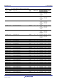
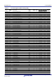

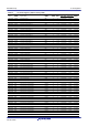
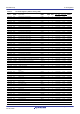
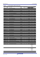
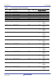
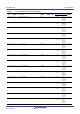

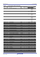
Table Of Contents
- Cover
- Notice
- General Precautions in the Handling of Microprocessing Unit and Microcontroller Unit Products
- How to Use This Manual
- Contents
- Features
- 1. Overview
- 2. CPU
- 2.1 Features
- 2.2 Register Set of the CPU
- 2.2.1 General-Purpose Registers (R0 to R15)
- 2.2.2 Control Registers
- 2.2.2.1 Interrupt Stack Pointer (ISP)/User Stack Pointer (USP)
- 2.2.2.2 Exception Table Register (EXTB)
- 2.2.2.3 Interrupt Table Register (INTB)
- 2.2.2.4 Program Counter (PC)
- 2.2.2.5 Processor Status Word (PSW)
- 2.2.2.6 Backup PC (BPC)
- 2.2.2.7 Backup PSW (BPSW)
- 2.2.2.8 Fast Interrupt Vector Register (FINTV)
- 2.2.2.9 Floating-Point Status Word (FPSW)
- 2.2.3 Accumulator
- 2.3 Processor Mode
- 2.4 Data Types
- 2.5 Endian
- 2.6 Vector Table
- 2.7 Operation of Instructions
- 2.8 Number of Cycles
- 3. Operating Modes
- 4. Address Space
- 5. I/O Registers
- 6. Resets
- 7. Option-Setting Memory (OFSM)
- 8. Voltage Detection Circuit (LVDAb)
- 9. Clock Generation Circuit
- 9.1 Overview
- 9.2 Register Descriptions
- 9.2.1 System Clock Control Register (SCKCR)
- 9.2.2 System Clock Control Register 3 (SCKCR3)
- 9.2.3 PLL Control Register (PLLCR)
- 9.2.4 PLL Control Register 2 (PLLCR2)
- 9.2.5 USB-dedicated PLL Control Register (UPLLCR)
- 9.2.6 USB-dedicated PLL Control Register 2 (UPLLCR2)
- 9.2.7 Main Clock Oscillator Control Register (MOSCCR)
- 9.2.8 Sub-Clock Oscillator Control Register (SOSCCR)
- 9.2.9 Low-Speed On-Chip Oscillator Control Register (LOCOCR)
- 9.2.10 IWDT-Dedicated On-Chip Oscillator Control Register (ILOCOCR)
- 9.2.11 High-Speed On-Chip Oscillator Control Register (HOCOCR)
- 9.2.12 High-Speed On-Chip Oscillator Control Register 2 (HOCOCR2)
- 9.2.13 Oscillation Stabilization Flag Register (OSCOVFSR)
- 9.2.14 Oscillation Stop Detection Control Register (OSTDCR)
- 9.2.15 Oscillation Stop Detection Status Register (OSTDSR)
- 9.2.16 Main Clock Oscillator Wait Control Register (MOSCWTCR)
- 9.2.17 CLKOUT Output Control Register (CKOCR)
- 9.2.18 Main Clock Oscillator Forced Oscillation Control Register (MOFCR)
- 9.2.19 Memory Wait Cycle Setting Register (MEMWAIT)
- 9.2.20 Low-Speed On-Chip Oscillator Trimming Register (LOCOTRR)
- 9.2.21 IWDT-Dedicated On-Chip Oscillator Trimming Register (ILOCOTRR)
- 9.2.22 High-Speed On-Chip Oscillator Trimming Register n (HOCOTRRn) (n = 0, 3)
- 9.3 Main Clock Oscillator
- 9.4 Sub-Clock Oscillator
- 9.5 Dedicated Clock Oscillator for Bluetooth
- 9.6 Oscillation Stop Detection Function
- 9.7 PLL Circuit
- 9.8 Internal Clock
- 9.9 Usage Notes
- 10. Clock Frequency Accuracy Measurement Circuit (CAC)
- 10.1 Overview
- 10.2 Register Descriptions
- 10.2.1 CAC Control Register 0 (CACR0)
- 10.2.2 CAC Control Register 1 (CACR1)
- 10.2.3 CAC Control Register 2 (CACR2)
- 10.2.4 CAC Interrupt Request Enable Register (CAICR)
- 10.2.5 CAC Status Register (CASTR)
- 10.2.6 CAC Upper-Limit Value Setting Register (CAULVR)
- 10.2.7 CAC Lower-Limit Value Setting Register (CALLVR)
- 10.2.8 CAC Counter Buffer Register (CACNTBR)
- 10.3 Operation
- 10.4 Interrupt Requests
- 10.5 Usage Notes
- 11. Low Power Consumption
- 11.1 Overview
- 11.2 Register Descriptions
- 11.2.1 Standby Control Register (SBYCR)
- 11.2.2 Module Stop Control Register A (MSTPCRA)
- 11.2.3 Module Stop Control Register B (MSTPCRB)
- 11.2.4 Module Stop Control Register C (MSTPCRC)
- 11.2.5 Module Stop Control Register D (MSTPCRD)
- 11.2.6 Operating Power Control Register (OPCCR)
- 11.2.7 Sub Operating Power Control Register (SOPCCR)
- 11.2.8 Sleep Mode Return Clock Source Switching Register (RSTCKCR)
- 11.3 Reducing Power Consumption by Switching Clock Signals
- 11.4 Module Stop Function
- 11.5 Function for Lower Operating Power Consumption
- 11.6 Low Power Consumption Modes
- 11.7 Usage Notes
- 12. Battery Backup Function
- 13. Register Write Protection Function
- 14. Exception Handling
- 15. Interrupt Controller (ICUb)
- 15.1 Overview
- 15.2 Register Descriptions
- 15.2.1 Interrupt Request Register n (IRn) (n = interrupt vector number)
- 15.2.2 Interrupt Request Enable Register m (IERm) (m = 02h to 1Fh)
- 15.2.3 Interrupt Source Priority Register n (IPRn) (n = interrupt vector number)
- 15.2.4 Fast Interrupt Set Register (FIR)
- 15.2.5 Software Interrupt Generation Register (SWINTR)
- 15.2.6 DTC Transfer Request Enable Register n (DTCERn) (n = interrupt vector number)
- 15.2.7 DMAC Trigger Select Register m (DMRSRm) (m = DMAC channel number)
- 15.2.8 IRQ Control Register i (IRQCRi) (i = 0, 1, and 4 to 7)
- 15.2.9 IRQ Pin Digital Filter Enable Register 0 (IRQFLTE0)
- 15.2.10 IRQ Pin Digital Filter Setting Register 0 (IRQFLTC0)
- 15.2.11 Non-Maskable Interrupt Status Register (NMISR)
- 15.2.12 Non-Maskable Interrupt Enable Register (NMIER)
- 15.2.13 Non-Maskable Interrupt Status Clear Register (NMICLR)
- 15.2.14 NMI Pin Interrupt Control Register (NMICR)
- 15.2.15 NMI Pin Digital Filter Enable Register (NMIFLTE)
- 15.2.16 NMI Pin Digital Filter Setting Register (NMIFLTC)
- 15.3 Vector Table
- 15.4 Interrupt Operation
- 15.5 Non-maskable Interrupt Operation
- 15.6 Return from Power-Down States
- 15.7 Usage Note
- 16. Buses
- 17. Memory-Protection Unit (MPU)
- 17.1 Overview
- 17.2 Register Descriptions
- 17.2.1 Region-n Start Page Number Register (RSPAGEn) (n = 0 to 7)
- 17.2.2 Region-n End Page Number Register (REPAGEn) (n = 0 to 7)
- 17.2.3 Memory-Protection Enable Register (MPEN)
- 17.2.4 Background Access Control Register (MPBAC)
- 17.2.5 Memory-Protection Error Status-Clearing Register (MPECLR)
- 17.2.6 Memory-Protection Error Status Register (MPESTS)
- 17.2.7 Data Memory-Protection Error Address Register (MPDEA)
- 17.2.8 Region Search Address Register (MPSA)
- 17.2.9 Region Search Operation Register (MPOPS)
- 17.2.10 Region Invalidation Operation Register (MPOPI)
- 17.2.11 Instruction-Hit Region Register (MHITI)
- 17.2.12 Data-Hit Region Register (MHITD)
- 17.3 Functions
- 17.4 Procedures for Using Memory Protection
- 18. DMA Controller (DMACA)
- 18.1 Overview
- 18.2 Register Descriptions
- 18.2.1 DMA Source Address Register (DMSAR)
- 18.2.2 DMA Destination Address Register (DMDAR)
- 18.2.3 DMA Transfer Count Register (DMCRA)
- 18.2.4 DMA Block Transfer Count Register (DMCRB)
- 18.2.5 DMA Transfer Mode Register (DMTMD)
- 18.2.6 DMA Interrupt Setting Register (DMINT)
- 18.2.7 DMA Address Mode Register (DMAMD)
- 18.2.8 DMA Offset Register (DMOFR)
- 18.2.9 DMA Transfer Enable Register (DMCNT)
- 18.2.10 DMA Software Start Register (DMREQ)
- 18.2.11 DMA Status Register (DMSTS)
- 18.2.12 DMA Activation Source Flag Control Register (DMCSL)
- 18.2.13 DMA Module Activation Register (DMAST)
- 18.3 Operation
- 18.4 Ending DMA Transfer
- 18.5 Interrupts
- 18.6 Event Link Function
- 18.7 Low Power Consumption Function
- 18.8 Usage Notes
- 18.8.1 DMA Transfer to Peripheral Modules
- 18.8.2 Access to the Registers during DMA Transfer
- 18.8.3 DMA Transfer to Reserved Areas
- 18.8.4 Interrupt Request by the DMA Activation Source Flag Control Register (DMCSL) at the End of each Transfer
- 18.8.5 Setting of DMAC Activation Source Select Register of the Interrupt Controller (ICU.DMRSRm)
- 18.8.6 Suspending or Restarting DMA Activation
- 19. Data Transfer Controller (DTCa)
- 19.1 Overview
- 19.2 Register Descriptions
- 19.2.1 DTC Mode Register A (MRA)
- 19.2.2 DTC Mode Register B (MRB)
- 19.2.3 DTC Transfer Source Register (SAR)
- 19.2.4 DTC Transfer Destination Register (DAR)
- 19.2.5 DTC Transfer Count Register A (CRA)
- 19.2.6 DTC Transfer Count Register B (CRB)
- 19.2.7 DTC Control Register (DTCCR)
- 19.2.8 DTC Vector Base Register (DTCVBR)
- 19.2.9 DTC Address Mode Register (DTCADMOD)
- 19.2.10 DTC Module Start Register (DTCST)
- 19.2.11 DTC Status Register (DTCSTS)
- 19.3 Request Sources
- 19.4 Operation

R01UH0823EJ0110 Rev.1.10 Page 126 of 1852
Nov 30, 2020
RX23W Group 5. I/O Registers
0008 C416h RTC Binary Counter 3 Alarm Register BCNT3AR 8 8 2 or 3 PCLKB 2 ICLK section 28.
0008 C418h RTC Date Alarm Register RDAYAR 8 8 2 or 3 PCLKB 2 ICLK section 28.
0008 C418h RTC Binary Counter 0 Alarm Enable Register BCNT0AER 8 8 2 or 3 PCLKB 2 ICLK section 28.
0008 C41Ah RTC Month Alarm Register RMONAR 8 8 2 or 3 PCLKB 2 ICLK section 28.
0008 C41Ah RTC Binary Counter 1 Alarm Enable Register BCNT1AER 8 8 2 or 3 PCLKB 2 ICLK section 28.
0008 C41Ch RTC Year Alarm Register RYRAR 16 16 2 or 3 PCLKB 2 ICLK section 28.
0008 C41Ch RTC Binary Counter 2 Alarm Enable Register BCNT2AER 16 16 2 or 3 PCLKB 2 ICLK section 28.
0008 C41Eh RTC Year Alarm Enable Register RYRAREN 8 8 2 or 3 PCLKB 2 ICLK section 28.
0008 C41Eh RTC Binary Counter 3 Alarm Enable Register BCNT3AER 8 8 2 or 3 PCLKB 2 ICLK section 28.
0008 C422h RTC RTC Control Register 1 RCR1 8 8 2 or 3 PCLKB 2 ICLK section 28.
0008 C424h RTC RTC Control Register 2 RCR2 8 8 2 or 3 PCLKB 2 ICLK section 28.
0008 C426h RTC RTC Control Register 3 RCR3 8 8 2 or 3 PCLKB 2 ICLK section 28.
0008 C42Eh RTC Time Error Adjustment Register RADJ 8 8 2 or 3 PCLKB 2 ICLK section 28.
0008 C440h RTC Time Capture Control Register 0 RTCCR0 8 8 2 or 3 PCLKB 2 ICLK section 28.
0008 C442h RTC Time Capture Control Register 1 RTCCR1 8 8 2 or 3 PCLKB 2 ICLK section 28.
0008 C452h RTC Second Capture Register 0 RSECCP0 8 8 2 or 3 PCLKB 2 ICLK section 28.
0008 C452h RTC BCNT0 Capture Register 0 BCNT0CP0 8 8 2 or 3 PCLKB 2 ICLK section 28.
0008 C454h RTC Minute Capture Register 0 RMINCP0 8 8 2 or 3 PCLKB 2 ICLK section 28.
0008 C454h RTC BCNT1 Capture Register 0 BCNT1CP0 8 8 2 or 3 PCLKB 2 ICLK section 28.
0008 C456h RTC Hour Capture Register 0 RHRCP0 8 8 2 or 3 PCLKB 2 ICLK section 28.
0008 C456h RTC BCNT2 Capture Register 0 BCNT2CP0 8 8 2 or 3 PCLKB 2 ICLK section 28.
0008 C45Ah RTC Date Capture Register 0 RDAYCP0 8 8 2 or 3 PCLKB 2 ICLK section 28.
0008 C45Ah RTC BCNT3 Capture Register 0 BCNT3CP0 8 8 2 or 3 PCLKB 2 ICLK section 28.
0008 C45Ch RTC Month Capture Register 0 RMONCP0 8 8 2 or 3 PCLKB 2 ICLK section 28.
0008 C462h RTC Second Capture Register 1 RSECCP1 8 8 2 or 3 PCLKB 2 ICLK section 28.
0008 C462h RTC BCNT0 Capture Register 1 BCNT0CP1 8 8 2 or 3 PCLKB 2 ICLK section 28.
0008 C464h RTC Minute Capture Register 1 RMINCP1 8 8 2 or 3 PCLKB 2 ICLK section 28.
0008 C464h RTC BCNT1 Capture Register 1 BCNT1CP1 8 8 2 or 3 PCLKB 2 ICLK section 28.
0008 C466h RTC Hour Capture Register 1 RHRCP1 8 8 2 or 3 PCLKB 2 ICLK section 28.
0008 C466h RTC BCNT2 Capture Register 1 BCNT2CP1 8 8 2 or 3 PCLKB 2 ICLK section 28.
0008 C46Ah RTC Date Capture Register 1 RDAYCP1 8 8 2 or 3 PCLKB 2 ICLK section 28.
0008 C46Ah RTC BCNT3 Capture Register 1 BCNT3CP1 8 8 2 or 3 PCLKB 2 ICLK section 28.
0008 C46Ch RTC Month Capture Register 1 RMONCP1 8 8 2 or 3 PCLKB 2 ICLK section 28.
0008 C5A0h CMPB Comparator B1 Control Register 1 CPB1CNT1 8 8 2 or 3 PCLKB 2 ICLK section 47.
0008 C5A1h CMPB Comparator B1 Control Register 2 CPB1CNT2 8 8 2 or 3 PCLKB 2 ICLK section 47.
0008 C5A2h CMPB Comparator B1 Flag Register CPB1FLG 8 8 2 or 3 PCLKB 2 ICLK section 47.
0008 C5A3h CMPB Comparator B1 Interrupt Control Register CPB1INT 8 8 2 or 3 PCLKB 2 ICLK section 47.
0008 C5A4h CMPB Comparator B1 Filter Select Register CPB1F 8 8 2 or 3 PCLKB 2 ICLK section 47.
0008 C5A5h CMPB Comparator B1 Mode Select Register CPB1MD 8 8 2 or 3 PCLKB 2 ICLK section 47.
0008 C5A6h CMPB Comparator B1 Reference Input Voltage Select Register CPB1REF 8 8 2 or 3 PCLKB 2 ICLK section 47.
0008 C5A7h CMPB Comparator B1 Output Control Register CPB1OCR 8 8 2 or 3 PCLKB 2 ICLK section 47.
000A 0000h USB0 System Configuration Control Register SYSCFG 16 16 3, 4 PCLKB 2 ICLK section 32.
000A 0004h USB0 System Configuration Status Register 0 SYSSTS0 16 16 9 PCLKB
or more
Rounded up to
the nearest
integer greater
than 1 + 9 ×
(frequency
ratio of ICLK/
PCLKB)*
2
section 32.
000A 0008h USB0 Device State Control Register 0 DVSTCTR0 16 16 9 PCLKB
or more
Rounded up to
the nearest
integer greater
than 1 + 9 ×
(frequency
ratio of ICLK/
PCLKB)*
2
section 32.
000A 0014h USB0 CFIFO Port Register CFIFO 16 16 3, 4 PCLKB 2 ICLK section 32.
Table 5.1 List of I/O Registers (Address Order) (17/31)
Address
Module
Symbol Register Name
Register
Symbol
Number
of Bits
Access
Size
Number of Access Cycles
Reference
SectionICLK ≥ PCLK ICLK <PCLK