
Product Info

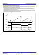


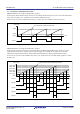

Table Of Contents
- 20. Event Link Controller (ELC)
- 20.1 Overview
- 20.2 Register Descriptions
- 20.2.1 Event Link Control Register (ELCR)
- 20.2.2 Event Link Setting Register n (ELSRn) (n = 1 to 4, 7, 8, 10, 12, 14 to 16, 18 to 29)
- 20.2.3 Event Link Option Setting Register A (ELOPA)
- 20.2.4 Event Link Option Setting Register B (ELOPB)
- 20.2.5 Event Link Option Setting Register C (ELOPC)
- 20.2.6 Event Link Option Setting Register D (ELOPD)
- 20.2.7 Port Group Setting Register n (PGRn) (n = 1, 2)
- 20.2.8 Port Group Control Register n (PGCn) (n = 1, 2)
- 20.2.9 Port Buffer Register n (PDBFn) (n = 1, 2)
- 20.2.10 Event Link Port Setting Register m (PELm) (m = 0 to 3)
- 20.2.11 Event Link Software Event Generation Register (ELSEGR)
- 20.3 Operation
- 20.3.1 Relation between Interrupt Handling and Event Linking
- 20.3.2 Event Linkage
- 20.3.3 Operation of Peripheral Timer Modules When Event Signal is Input
- 20.3.4 Operation of CTSU When Event Signal is Input
- 20.3.5 Operation of A/D and D/A Converters When Event Signal is Input
- 20.3.6 I/O Port Operation When Event Signal is Input and Event Generation
- 20.3.7 Example of Procedure for Linking Events
- 20.4 Usage Notes
- 21. I/O Ports
- 21.1 Overview
- 21.2 I/O Port Configuration
- 21.3 Register Descriptions
- 21.3.1 Port Direction Register (PDR)
- 21.3.2 Port Output Data Register (PODR)
- 21.3.3 Port Input Data Register (PIDR)
- 21.3.4 Port Mode Register (PMR)
- 21.3.5 Open Drain Control Register 0 (ODR0)
- 21.3.6 Open Drain Control Register 1 (ODR1)
- 21.3.7 Pull-Up Control Register (PCR)
- 21.3.8 Drive Capacity Control Register (DSCR)
- 21.4 Initialization of the Port Direction Register (PDR)
- 21.5 Handling of Unused Pins
- 22. Multi-Function Pin Controller (MPC)
- 22.1 Overview
- 22.2 Register Descriptions
- 22.2.1 Write-Protect Register (PWPR)
- 22.2.2 P0n Pin Function Control Register (P0nPFS) (n = 3, 5, 7)
- 22.2.3 P1n Pin Function Control Registers (P1nPFS) (n = 4 to 7)
- 22.2.4 P2n Pin Function Control Register (P2nPFS) (n = 1, 2, 5 to 7)
- 22.2.5 P3n Pin Function Control Registers (P3nPFS) (n = 0, 1)
- 22.2.6 P4n Pin Function Control Registers (P4nPFS) (n = 0 to 7)
- 22.2.7 PBn Pin Function Control Registers (PBnPFS) (n = 0, 1, 3, 5, 7)
- 22.2.8 PCn Pin Function Control Registers (PCnPFS) (n = 0, 2 to 7)
- 22.2.9 PDn Pin Function Control Registers (PDnPFS) (n = 3)
- 22.2.10 PEn Pin Function Control Registers (PEnPFS) (n = 0 to 4)
- 22.2.11 PJn Pin Function Control Registers (PJnPFS) (n = 3)
- 22.3 Usage Notes
- 23. Multi-Function Timer Pulse Unit 2 (MTU2a)
- 23.1 Overview
- 23.2 Register Descriptions
- 23.2.1 Timer Control Register (TCR)
- 23.2.2 Timer Mode Register (TMDR)
- 23.2.3 Timer I/O Control Register (TIOR)
- 23.2.4 Timer Interrupt Enable Register (TIER)
- 23.2.5 Timer Status Register (TSR)
- 23.2.6 Timer Buffer Operation Transfer Mode Register (TBTM)
- 23.2.7 Timer Input Capture Control Register (TICCR)
- 23.2.8 Timer A/D Converter Start Request Control Register (TADCR)
- 23.2.9 Timer A/D Converter Start Request Cycle Set Registers A and B (TADCORA and TADCORB)
- 23.2.10 Timer A/D Converter Start Request Cycle Set Buffer Registers A and B (TADCOBRA and TADCOBRB)
- 23.2.11 Timer Counter (TCNT)
- 23.2.12 Timer General Register (TGR)
- 23.2.13 Timer Start Register (TSTR)
- 23.2.14 Timer Synchronous Register (TSYR)
- 23.2.15 Timer Read/Write Enable Register (TRWER)
- 23.2.16 Timer Output Master Enable Register (TOER)
- 23.2.17 Timer Output Control Register 1 (TOCR1)
- 23.2.18 Timer Output Control Register 2 (TOCR2)
- 23.2.19 Timer Output Level Buffer Register (TOLBR)
- 23.2.20 Timer Gate Control Register (TGCR)
- 23.2.21 Timer Subcounter (TCNTS)
- 23.2.22 Timer Dead Time Data Register (TDDR)
- 23.2.23 Timer Cycle Data Register (TCDR)
- 23.2.24 Timer Cycle Buffer Register (TCBR)
- 23.2.25 Timer Interrupt Skipping Set Register (TITCR)
- 23.2.26 Timer Interrupt Skipping Counter (TITCNT)
- 23.2.27 Timer Buffer Transfer Set Register (TBTER)
- 23.2.28 Timer Dead Time Enable Register (TDER)
- 23.2.29 Timer Waveform Control Register (TWCR)
- 23.2.30 Noise Filter Control Registers (NFCR)
- 23.2.31 Bus Master Interface
- 23.3 Operation
- 23.4 Interrupt Sources
- 23.5 Operation Timing
- 23.6 Usage Notes
- 23.6.1 Module Clock Stop Mode Setting
- 23.6.2 Count Clock Restrictions
- 23.6.3 Notes on Cycle Setting
- 23.6.4 Contention between TCNT Write and Clear Operations
- 23.6.5 Contention between TCNT Write and Increment Operations
- 23.6.6 Contention between TGR Write Operation and Compare Match
- 23.6.7 Contention between Buffer Register Write Operation and Compare Match
- 23.6.8 Contention between Buffer Register Write and TCNT Clear Operations
- 23.6.9 Contention between TGR Read Operation and Input Capture
- 23.6.10 Contention between TGR Write Operation and Input Capture
- 23.6.11 Contention between Buffer Register Write Operation and Input Capture
- 23.6.12 Contention between MTU2.TCNT Write Operation and Overflow/Underflow in Cascaded Operation
- 23.6.13 Counter Value When Count Operation is Stopped in Complementary PWM Mode
- 23.6.14 Buffer Operation Setting in Complementary PWM Mode
- 23.6.15 Buffer Operation and Compare Match Flags in Reset-Synchronized PWM Mode
- 23.6.16 Overflow Flags in Reset-Synchronized PWM Mode
- 23.6.17 Contention between Overflow/Underflow and Counter Clearing
- 23.6.18 Contention between TCNT Write Operation and Overflow/Underflow
- 23.6.19 Notes on Transition from Normal Mode or PWM Mode 1 to Reset-Synchronized PWM Mode
- 23.6.20 Output Level in Complementary PWM Mode or Reset-Synchronized PWM Mode
- 23.6.21 Interrupts during Periods in the Module Stop State
- 23.6.22 Simultaneous Input Capture in MTU1.TCNT and MTU2.TCNT in Cascade Connection
- 23.6.23 Notes When Complementary PWM Mode Output Protection Functions are Not Used
- 23.6.24 Points for Caution to Prevent Malfunctions in Synchronous Clearing for Complementary PWM Mode
- 23.6.25 Continuous Output of Interrupt Signal in Response to a Compare Match
- 23.6.26 Usage Notes on A/D Converter Delaying Function in Complementary PWM Mode
- 23.7 MTU Output Pin Initialization
- 23.8 Operations Linked by the ELC
- 24. Port Output Enable 2 (POE2a)
- 24.1 Overview
- 24.2 Register Descriptions
- 24.2.1 Input Level Control/Status Register 1 (ICSR1)
- 24.2.2 Output Level Control/Status Register 1 (OCSR1)
- 24.2.3 Input Level Control/Status Register 2 (ICSR2)
- 24.2.4 Software Port Output Enable Register (SPOER)
- 24.2.5 Port Output Enable Control Register 1 (POECR1)
- 24.2.6 Port Output Enable Control Register 2 (POECR2)
- 24.2.7 Input Level Control/Status Register 3 (ICSR3)
- 24.3 Operation
- 24.3.1 Input Level Detection Operation
- 24.3.2 Output-Level Compare Operation
- 24.3.3 High-Impedance Control Using Registers
- 24.3.4 High-Impedance Control on Detection of Stopped Oscillation
- 24.3.5 High-Impedance Control in Response to Receiving an Event Signal from the ELC
- 24.3.6 Release from the High-Impedance
- 24.4 Interrupts
- 24.5 Usage Notes
- 25. 16-Bit Timer Pulse Unit (TPUa)
- 25.1 Overview
- 25.2 Register Descriptions
- 25.2.1 Timer Control Register (TCR)
- 25.2.2 Timer Mode Register (TMDR)
- 25.2.3 Timer I/O Control Register (TIORH, TIORL, TIOR)
- 25.2.4 Timer Interrupt Enable Register (TIER)
- 25.2.5 Timer Status Register (TSR)
- 25.2.6 Timer Counter (TCNT)
- 25.2.7 Timer General Register A (TGRA), Timer General Register B (TGRB), Timer General Register C (TGRC), Timer General Register D (TGRD)
- 25.2.8 Timer Start Register (TSTR)
- 25.2.9 Timer Synchronous Register (TSYR)
- 25.2.10 Noise Filter Control Register (NFCR)
- 25.3 Operation
- 25.4 Interrupt Sources
- 25.5 DTC Activation
- 25.6 DMAC Activation
- 25.7 A/D Converter Activation
- 25.8 Operation Timing
- 25.9 Usage Notes
- 25.9.1 Module Stop Function Setting
- 25.9.2 Input Clock Restrictions
- 25.9.3 Notes on Cycle Setting
- 25.9.4 Conflict between TPUm.TCNT Write and Clear Operations
- 25.9.5 Conflict between TPUm.TCNT Write and Increment Operations
- 25.9.6 Conflict between TPUm.TGRy Write and Compare Match
- 25.9.7 Conflict between Buffer Register Write and Compare Match
- 25.9.8 Conflict between TPUm.TGRy Read and Input Capture
- 25.9.9 Conflict between TPUm.TGRy Write and Input Capture
- 25.9.10 Conflict between Buffer Register Write and Input Capture
- 25.9.11 TCNT Simultaneous Input Capture in Cascade Operation
- 25.9.12 Conflict between Overflow/Underflow and Counter Clearing
- 25.9.13 Conflict between TPUm.TCNT Write and Overflow/Underflow
- 25.9.14 Multiplexing of I/O Pins
- 25.9.15 Continuous Output of Compare-Match Pulse Interrupt Signal
- 25.9.16 Continuous Output of Input-Capture Pulse Interrupt Signal
- 25.9.17 Continuous Output of Underflow Pulse Interrupt Signal
- 26. 8-Bit Timer (TMR)
- 26.1 Overview
- 26.2 Register Descriptions
- 26.3 Operation
- 26.4 Operation Timing
- 26.5 Operation with Cascaded Connection
- 26.6 Interrupt Sources
- 26.7 Link Operation by ELC
- 26.8 Usage Notes
- 26.8.1 Module Stop State Setting
- 26.8.2 Notes on Setting Cycle
- 26.8.3 Conflict between TCNT Write and Counter Clear
- 26.8.4 Conflict between TCNT Write and Increment
- 26.8.5 Conflict between TCORA or TCORB Write and Compare Match
- 26.8.6 Conflict between Compare Matches A and B
- 26.8.7 Switching of Internal Clocks and TCNT Operation
- 26.8.8 Clock Source Setting with Cascaded Connection
- 26.8.9 Continuous Output of Compare Match Interrupt Signal
- 27. Compare Match Timer (CMT)
- 28. Realtime Clock (RTCe)
- 28.1 Overview
- 28.2 Register Descriptions
- 28.2.1 64-Hz Counter (R64CNT)
- 28.2.2 Second Counter (RSECCNT)/Binary Counter 0 (BCNT0)
- 28.2.3 Minute Counter (RMINCNT)/Binary Counter 1 (BCNT1)
- 28.2.4 Hour Counter (RHRCNT)/Binary Counter 2 (BCNT2)
- 28.2.5 Day-of-Week Counter (RWKCNT)/Binary Counter 3 (BCNT3)
- 28.2.6 Date Counter (RDAYCNT)
- 28.2.7 Month Counter (RMONCNT)
- 28.2.8 Year Counter (RYRCNT)
- 28.2.9 Second Alarm Register (RSECAR)/Binary Counter 0 Alarm Register (BCNT0AR)
- 28.2.10 Minute Alarm Register (RMINAR)/Binary Counter 1 Alarm Register (BCNT1AR)
- 28.2.11 Hour Alarm Register (RHRAR)/Binary Counter 2 Alarm Register (BCNT2AR)
- 28.2.12 Day-of-Week Alarm Register (RWKAR)/Binary Counter 3 Alarm Register (BCNT3AR)
- 28.2.13 Date Alarm Register (RDAYAR)/Binary Counter 0 Alarm Enable Register (BCNT0AER)
- 28.2.14 Month Alarm Register (RMONAR)/Binary Counter 1 Alarm Enable Register (BCNT1AER)
- 28.2.15 Year Alarm Register (RYRAR)/Binary Counter 2 Alarm Enable Register (BCNT2AER)
- 28.2.16 Year Alarm Enable Register (RYRAREN)/Binary Counter 3 Alarm Enable Register (BCNT3AER)
- 28.2.17 RTC Control Register 1 (RCR1)
- 28.2.18 RTC Control Register 2 (RCR2)
- 28.2.19 RTC Control Register 3 (RCR3)
- 28.2.20 Time Error Adjustment Register (RADJ)
- 28.2.21 Time Capture Control Register n (RTCCRn) (n = 0, 1)
- 28.2.22 Second Capture Register n (RSECCPn) (n = 0, 1)/BCNT0 Capture Register n (BCNT0CPn) (n = 0, 1)
- 28.2.23 Minute Capture Register n (RMINCPn) (n = 0, 1)/BCNT1 Capture Register n (BCNT1CPn) (n = 0, 1)
- 28.2.24 Hour Capture Register n (RHRCPn) (n = 0, 1)/BCNT2 Capture Register n (BCNT2CPn) (n = 0, 1)
- 28.2.25 Date Capture Register n (RDAYCPn) (n = 0, 1)/BCNT3 Capture Register n (BCNT3CPn) (n = 0, 1)
- 28.2.26 Month Capture Register n (RMONCPn) (n = 0, 1)

R01UH0823EJ0110 Rev.1.10 Page 705 of 1852
Nov 30, 2020
RX23W Group 25. 16-Bit Timer Pulse Unit (TPUa)
The correspondence between PWM output pins and registers is listed in Table 25.22.
Note: In PWM mode 2, PWM waveform output is not possible for the TPUm.TGRy register in which the cycle is set.
Table 25.22 PWM Output Registers and Output Pins
Channel Register
Output Pin
PWM Mode 1 PWM Mode 2
TPU0 TPU0.TGRA No pin is assigned for this output. No pin is assigned for this output.
TPU0.TGRB TIOCB0
TPU0.TGRC No pin is assigned for this output. No pin is assigned for this output.
TPU0.TGRD No pin is assigned for this output.
TPU1 TPU1.TGRA No pin is assigned for this output. No pin is assigned for this output.
TPU1.TGRB TIOCB1
TPU2 TPU2.TGRA No pin is assigned for this output. No pin is assigned for this output.
TPU2.TGRB TIOCB2
TPU3 TPU3.TGRA TIOCA3 TIOCA3
TPU3.TGRB TIOCB3
TPU3.TGRC TIOCC3 TIOCC3
TPU3.TGRD TIOCD3
TPU4 TPU4.TGRA TIOCA4 TIOCA4
TPU4.TGRB TIOCB4
TPU5 TPU5.TGRA No pin is assigned for this output. No pin is assigned for this output.
TPU5.TGRB TIOCB5