
Product Info
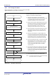


Table Of Contents
- 20. Event Link Controller (ELC)
- 20.1 Overview
- 20.2 Register Descriptions
- 20.2.1 Event Link Control Register (ELCR)
- 20.2.2 Event Link Setting Register n (ELSRn) (n = 1 to 4, 7, 8, 10, 12, 14 to 16, 18 to 29)
- 20.2.3 Event Link Option Setting Register A (ELOPA)
- 20.2.4 Event Link Option Setting Register B (ELOPB)
- 20.2.5 Event Link Option Setting Register C (ELOPC)
- 20.2.6 Event Link Option Setting Register D (ELOPD)
- 20.2.7 Port Group Setting Register n (PGRn) (n = 1, 2)
- 20.2.8 Port Group Control Register n (PGCn) (n = 1, 2)
- 20.2.9 Port Buffer Register n (PDBFn) (n = 1, 2)
- 20.2.10 Event Link Port Setting Register m (PELm) (m = 0 to 3)
- 20.2.11 Event Link Software Event Generation Register (ELSEGR)
- 20.3 Operation
- 20.3.1 Relation between Interrupt Handling and Event Linking
- 20.3.2 Event Linkage
- 20.3.3 Operation of Peripheral Timer Modules When Event Signal is Input
- 20.3.4 Operation of CTSU When Event Signal is Input
- 20.3.5 Operation of A/D and D/A Converters When Event Signal is Input
- 20.3.6 I/O Port Operation When Event Signal is Input and Event Generation
- 20.3.7 Example of Procedure for Linking Events
- 20.4 Usage Notes
- 21. I/O Ports
- 21.1 Overview
- 21.2 I/O Port Configuration
- 21.3 Register Descriptions
- 21.3.1 Port Direction Register (PDR)
- 21.3.2 Port Output Data Register (PODR)
- 21.3.3 Port Input Data Register (PIDR)
- 21.3.4 Port Mode Register (PMR)
- 21.3.5 Open Drain Control Register 0 (ODR0)
- 21.3.6 Open Drain Control Register 1 (ODR1)
- 21.3.7 Pull-Up Control Register (PCR)
- 21.3.8 Drive Capacity Control Register (DSCR)
- 21.4 Initialization of the Port Direction Register (PDR)
- 21.5 Handling of Unused Pins
- 22. Multi-Function Pin Controller (MPC)
- 22.1 Overview
- 22.2 Register Descriptions
- 22.2.1 Write-Protect Register (PWPR)
- 22.2.2 P0n Pin Function Control Register (P0nPFS) (n = 3, 5, 7)
- 22.2.3 P1n Pin Function Control Registers (P1nPFS) (n = 4 to 7)
- 22.2.4 P2n Pin Function Control Register (P2nPFS) (n = 1, 2, 5 to 7)
- 22.2.5 P3n Pin Function Control Registers (P3nPFS) (n = 0, 1)
- 22.2.6 P4n Pin Function Control Registers (P4nPFS) (n = 0 to 7)
- 22.2.7 PBn Pin Function Control Registers (PBnPFS) (n = 0, 1, 3, 5, 7)
- 22.2.8 PCn Pin Function Control Registers (PCnPFS) (n = 0, 2 to 7)
- 22.2.9 PDn Pin Function Control Registers (PDnPFS) (n = 3)
- 22.2.10 PEn Pin Function Control Registers (PEnPFS) (n = 0 to 4)
- 22.2.11 PJn Pin Function Control Registers (PJnPFS) (n = 3)
- 22.3 Usage Notes
- 23. Multi-Function Timer Pulse Unit 2 (MTU2a)
- 23.1 Overview
- 23.2 Register Descriptions
- 23.2.1 Timer Control Register (TCR)
- 23.2.2 Timer Mode Register (TMDR)
- 23.2.3 Timer I/O Control Register (TIOR)
- 23.2.4 Timer Interrupt Enable Register (TIER)
- 23.2.5 Timer Status Register (TSR)
- 23.2.6 Timer Buffer Operation Transfer Mode Register (TBTM)
- 23.2.7 Timer Input Capture Control Register (TICCR)
- 23.2.8 Timer A/D Converter Start Request Control Register (TADCR)
- 23.2.9 Timer A/D Converter Start Request Cycle Set Registers A and B (TADCORA and TADCORB)
- 23.2.10 Timer A/D Converter Start Request Cycle Set Buffer Registers A and B (TADCOBRA and TADCOBRB)
- 23.2.11 Timer Counter (TCNT)
- 23.2.12 Timer General Register (TGR)
- 23.2.13 Timer Start Register (TSTR)
- 23.2.14 Timer Synchronous Register (TSYR)
- 23.2.15 Timer Read/Write Enable Register (TRWER)
- 23.2.16 Timer Output Master Enable Register (TOER)
- 23.2.17 Timer Output Control Register 1 (TOCR1)
- 23.2.18 Timer Output Control Register 2 (TOCR2)
- 23.2.19 Timer Output Level Buffer Register (TOLBR)
- 23.2.20 Timer Gate Control Register (TGCR)
- 23.2.21 Timer Subcounter (TCNTS)
- 23.2.22 Timer Dead Time Data Register (TDDR)
- 23.2.23 Timer Cycle Data Register (TCDR)
- 23.2.24 Timer Cycle Buffer Register (TCBR)
- 23.2.25 Timer Interrupt Skipping Set Register (TITCR)
- 23.2.26 Timer Interrupt Skipping Counter (TITCNT)
- 23.2.27 Timer Buffer Transfer Set Register (TBTER)
- 23.2.28 Timer Dead Time Enable Register (TDER)
- 23.2.29 Timer Waveform Control Register (TWCR)
- 23.2.30 Noise Filter Control Registers (NFCR)
- 23.2.31 Bus Master Interface
- 23.3 Operation
- 23.4 Interrupt Sources
- 23.5 Operation Timing
- 23.6 Usage Notes
- 23.6.1 Module Clock Stop Mode Setting
- 23.6.2 Count Clock Restrictions
- 23.6.3 Notes on Cycle Setting
- 23.6.4 Contention between TCNT Write and Clear Operations
- 23.6.5 Contention between TCNT Write and Increment Operations
- 23.6.6 Contention between TGR Write Operation and Compare Match
- 23.6.7 Contention between Buffer Register Write Operation and Compare Match
- 23.6.8 Contention between Buffer Register Write and TCNT Clear Operations
- 23.6.9 Contention between TGR Read Operation and Input Capture
- 23.6.10 Contention between TGR Write Operation and Input Capture
- 23.6.11 Contention between Buffer Register Write Operation and Input Capture
- 23.6.12 Contention between MTU2.TCNT Write Operation and Overflow/Underflow in Cascaded Operation
- 23.6.13 Counter Value When Count Operation is Stopped in Complementary PWM Mode
- 23.6.14 Buffer Operation Setting in Complementary PWM Mode
- 23.6.15 Buffer Operation and Compare Match Flags in Reset-Synchronized PWM Mode
- 23.6.16 Overflow Flags in Reset-Synchronized PWM Mode
- 23.6.17 Contention between Overflow/Underflow and Counter Clearing
- 23.6.18 Contention between TCNT Write Operation and Overflow/Underflow
- 23.6.19 Notes on Transition from Normal Mode or PWM Mode 1 to Reset-Synchronized PWM Mode
- 23.6.20 Output Level in Complementary PWM Mode or Reset-Synchronized PWM Mode
- 23.6.21 Interrupts during Periods in the Module Stop State
- 23.6.22 Simultaneous Input Capture in MTU1.TCNT and MTU2.TCNT in Cascade Connection
- 23.6.23 Notes When Complementary PWM Mode Output Protection Functions are Not Used
- 23.6.24 Points for Caution to Prevent Malfunctions in Synchronous Clearing for Complementary PWM Mode
- 23.6.25 Continuous Output of Interrupt Signal in Response to a Compare Match
- 23.6.26 Usage Notes on A/D Converter Delaying Function in Complementary PWM Mode
- 23.7 MTU Output Pin Initialization
- 23.8 Operations Linked by the ELC
- 24. Port Output Enable 2 (POE2a)
- 24.1 Overview
- 24.2 Register Descriptions
- 24.2.1 Input Level Control/Status Register 1 (ICSR1)
- 24.2.2 Output Level Control/Status Register 1 (OCSR1)
- 24.2.3 Input Level Control/Status Register 2 (ICSR2)
- 24.2.4 Software Port Output Enable Register (SPOER)
- 24.2.5 Port Output Enable Control Register 1 (POECR1)
- 24.2.6 Port Output Enable Control Register 2 (POECR2)
- 24.2.7 Input Level Control/Status Register 3 (ICSR3)
- 24.3 Operation
- 24.3.1 Input Level Detection Operation
- 24.3.2 Output-Level Compare Operation
- 24.3.3 High-Impedance Control Using Registers
- 24.3.4 High-Impedance Control on Detection of Stopped Oscillation
- 24.3.5 High-Impedance Control in Response to Receiving an Event Signal from the ELC
- 24.3.6 Release from the High-Impedance
- 24.4 Interrupts
- 24.5 Usage Notes
- 25. 16-Bit Timer Pulse Unit (TPUa)
- 25.1 Overview
- 25.2 Register Descriptions
- 25.2.1 Timer Control Register (TCR)
- 25.2.2 Timer Mode Register (TMDR)
- 25.2.3 Timer I/O Control Register (TIORH, TIORL, TIOR)
- 25.2.4 Timer Interrupt Enable Register (TIER)
- 25.2.5 Timer Status Register (TSR)
- 25.2.6 Timer Counter (TCNT)
- 25.2.7 Timer General Register A (TGRA), Timer General Register B (TGRB), Timer General Register C (TGRC), Timer General Register D (TGRD)
- 25.2.8 Timer Start Register (TSTR)
- 25.2.9 Timer Synchronous Register (TSYR)
- 25.2.10 Noise Filter Control Register (NFCR)
- 25.3 Operation
- 25.4 Interrupt Sources
- 25.5 DTC Activation
- 25.6 DMAC Activation
- 25.7 A/D Converter Activation
- 25.8 Operation Timing
- 25.9 Usage Notes
- 25.9.1 Module Stop Function Setting
- 25.9.2 Input Clock Restrictions
- 25.9.3 Notes on Cycle Setting
- 25.9.4 Conflict between TPUm.TCNT Write and Clear Operations
- 25.9.5 Conflict between TPUm.TCNT Write and Increment Operations
- 25.9.6 Conflict between TPUm.TGRy Write and Compare Match
- 25.9.7 Conflict between Buffer Register Write and Compare Match
- 25.9.8 Conflict between TPUm.TGRy Read and Input Capture
- 25.9.9 Conflict between TPUm.TGRy Write and Input Capture
- 25.9.10 Conflict between Buffer Register Write and Input Capture
- 25.9.11 TCNT Simultaneous Input Capture in Cascade Operation
- 25.9.12 Conflict between Overflow/Underflow and Counter Clearing
- 25.9.13 Conflict between TPUm.TCNT Write and Overflow/Underflow
- 25.9.14 Multiplexing of I/O Pins
- 25.9.15 Continuous Output of Compare-Match Pulse Interrupt Signal
- 25.9.16 Continuous Output of Input-Capture Pulse Interrupt Signal
- 25.9.17 Continuous Output of Underflow Pulse Interrupt Signal
- 26. 8-Bit Timer (TMR)
- 26.1 Overview
- 26.2 Register Descriptions
- 26.3 Operation
- 26.4 Operation Timing
- 26.5 Operation with Cascaded Connection
- 26.6 Interrupt Sources
- 26.7 Link Operation by ELC
- 26.8 Usage Notes
- 26.8.1 Module Stop State Setting
- 26.8.2 Notes on Setting Cycle
- 26.8.3 Conflict between TCNT Write and Counter Clear
- 26.8.4 Conflict between TCNT Write and Increment
- 26.8.5 Conflict between TCORA or TCORB Write and Compare Match
- 26.8.6 Conflict between Compare Matches A and B
- 26.8.7 Switching of Internal Clocks and TCNT Operation
- 26.8.8 Clock Source Setting with Cascaded Connection
- 26.8.9 Continuous Output of Compare Match Interrupt Signal
- 27. Compare Match Timer (CMT)
- 28. Realtime Clock (RTCe)
- 28.1 Overview
- 28.2 Register Descriptions
- 28.2.1 64-Hz Counter (R64CNT)
- 28.2.2 Second Counter (RSECCNT)/Binary Counter 0 (BCNT0)
- 28.2.3 Minute Counter (RMINCNT)/Binary Counter 1 (BCNT1)
- 28.2.4 Hour Counter (RHRCNT)/Binary Counter 2 (BCNT2)
- 28.2.5 Day-of-Week Counter (RWKCNT)/Binary Counter 3 (BCNT3)
- 28.2.6 Date Counter (RDAYCNT)
- 28.2.7 Month Counter (RMONCNT)
- 28.2.8 Year Counter (RYRCNT)
- 28.2.9 Second Alarm Register (RSECAR)/Binary Counter 0 Alarm Register (BCNT0AR)
- 28.2.10 Minute Alarm Register (RMINAR)/Binary Counter 1 Alarm Register (BCNT1AR)
- 28.2.11 Hour Alarm Register (RHRAR)/Binary Counter 2 Alarm Register (BCNT2AR)
- 28.2.12 Day-of-Week Alarm Register (RWKAR)/Binary Counter 3 Alarm Register (BCNT3AR)
- 28.2.13 Date Alarm Register (RDAYAR)/Binary Counter 0 Alarm Enable Register (BCNT0AER)
- 28.2.14 Month Alarm Register (RMONAR)/Binary Counter 1 Alarm Enable Register (BCNT1AER)
- 28.2.15 Year Alarm Register (RYRAR)/Binary Counter 2 Alarm Enable Register (BCNT2AER)
- 28.2.16 Year Alarm Enable Register (RYRAREN)/Binary Counter 3 Alarm Enable Register (BCNT3AER)
- 28.2.17 RTC Control Register 1 (RCR1)
- 28.2.18 RTC Control Register 2 (RCR2)
- 28.2.19 RTC Control Register 3 (RCR3)
- 28.2.20 Time Error Adjustment Register (RADJ)
- 28.2.21 Time Capture Control Register n (RTCCRn) (n = 0, 1)
- 28.2.22 Second Capture Register n (RSECCPn) (n = 0, 1)/BCNT0 Capture Register n (BCNT0CPn) (n = 0, 1)
- 28.2.23 Minute Capture Register n (RMINCPn) (n = 0, 1)/BCNT1 Capture Register n (BCNT1CPn) (n = 0, 1)
- 28.2.24 Hour Capture Register n (RHRCPn) (n = 0, 1)/BCNT2 Capture Register n (BCNT2CPn) (n = 0, 1)
- 28.2.25 Date Capture Register n (RDAYCPn) (n = 0, 1)/BCNT3 Capture Register n (BCNT3CPn) (n = 0, 1)
- 28.2.26 Month Capture Register n (RMONCPn) (n = 0, 1)

R01UH0823EJ0110 Rev.1.10 Page 412 of 1852
Nov 30, 2020
RX23W Group 19. Data Transfer Controller (DTCa)
19.6 Examples of DTC Usage
19.6.1 Normal Transfer
As an example of DTC usage, its employment in the reception of 128 bytes of data by an SCI is described below.
(1) Transfer Information Setting
Set the MRA.MD[1:0] bits to 00b (normal transfer mode), the MRA.SZ[1:0] bits to 00b (byte transfer), and the
MRA.SM[1:0] bits to 00b (source address is fixed). Set the MRB.CHNE bit to 0 (chain transfer is disabled), the
MRB.DISEL bit to 0 (an interrupt request to the CPU is generated on completion of the specified number of data
transfers), and the MRB.DM[1:0] bits to 10b (DAR is incremented after data transfer). The MRB.DTS bit can be set to
any value. Set the RDR register address of the SCI in the SAR register, the start address of the RAM area for data storage
in the DAR register, and 128 (0080h) in the CRA register. The CRB register can be set to any value.
(2) DTC Vector Table Setting
The start address of the transfer information for the RXI interrupt is set in the vector table for the DTC.
(3) ICU Setting and DTC Module Activation
Set the corresponding ICU.DTCERn.DTCE bit to 1 and the ICU.IERm.IENj bit to 1.
Set the DTCST.DTCST bit to 1.
(4) SCI Setting
Enable the RXI interrupt by setting the SCR.RIE bit in the SCI to 1. If a reception error occurs during the SCI receive
operation, further reception is not performed. Accordingly, make settings so that the CPU can accept receive error
interrupts.
(5) DTC Transfer
Every time the reception of 1 byte by the SCI is completed, an RXI interrupt is generated to start the data transfer. The
DTC transfers the received byte from the RDR of the SCI to RAM, after which the DAR register is incremented and the
CRA register is decremented.
(6) Interrupt Handling
After 128 times of data transfers have been completed and the value in the CRA register becomes 0, an RXI interrupt
request is output to the CPU. Complete the process in the handling routine for this interrupt.