
How-To Guide
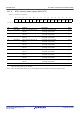
Table Of Contents
- 29. Low-Power Timer (LPT)
- 29.1 Overview
- 29.2 Register Descriptions
- 29.2.1 Low-Power Timer Control Register 1 (LPTCR1)
- 29.2.2 Low-Power Timer Control Register 2 (LPTCR2)
- 29.2.3 Low-Power Timer Control Register 3 (LPTCR3)
- 29.2.4 Low-Power Timer Period Setting Register (LPTPRD)
- 29.2.5 Low-Power Timer Compare Register 0 (LPCMR0)
- 29.2.6 Low-Power Timer Standby Wakeup Enable Register (LPWUCR)
- 29.3 Operation
- 29.4 Wakeup from Software Standby Mode by an Interrupt through the Event Link Controller (ELC)
- 29.5 Usage Notes
- 30. Watchdog Timer (WDTA)
- 30.1 Overview
- 30.2 Register Descriptions
- 30.3 Operation
- 31. Independent Watchdog Timer (IWDTa)
- 31.1 Overview
- 31.2 Register Descriptions
- 31.3 Operation
- 31.3.1 Count Operation in Each Start Mode
- 31.3.2 Control over Writing to the IWDTCR, IWDTRCR, and IWDTCSTPR Registers
- 31.3.3 Refresh Operation
- 31.3.4 Status Flags
- 31.3.5 Reset Output
- 31.3.6 Interrupt Sources
- 31.3.7 Reading the Counter Value
- 31.3.8 Correspondence between Option Function Select Register 0 (OFS0) and IWDT Registers
- 31.4 Link Operation by ELC
- 31.5 Usage Notes
- 32. USB 2.0 Host/Function Module (USBc)
- 32.1 Overview
- 32.2 Register Descriptions
- 32.2.1 System Configuration Control Register (SYSCFG)
- 32.2.2 System Configuration Status Register 0 (SYSSTS0)
- 32.2.3 Device State Control Register 0 (DVSTCTR0)
- 32.2.4 CFIFO Port Register (CFIFO), D0FIFO Port Register (D0FIFO), D1FIFO Port Register (D1FIFO)
- 32.2.5 CFIFO Port Select Register (CFIFOSEL), D0FIFO Port Select Register (D0FIFOSEL), D1FIFO Port Select Register (D1FIFOSEL)
- 32.2.6 CFIFO Port Control Register (CFIFOCTR), D0FIFO Port Control Register (D0FIFOCTR), D1FIFO Port Control Register (D1FIFOCTR)
- 32.2.7 Interrupt Enable Register 0 (INTENB0)
- 32.2.8 Interrupt Enable Register 1 (INTENB1)
- 32.2.9 BRDY Interrupt Enable Register (BRDYENB)
- 32.2.10 NRDY Interrupt Enable Register (NRDYENB)
- 32.2.11 BEMP Interrupt Enable Register (BEMPENB)
- 32.2.12 SOF Output Configuration Register (SOFCFG)
- 32.2.13 Interrupt Status Register 0 (INTSTS0)
- 32.2.14 Interrupt Status Register 1 (INTSTS1)
- 32.2.15 BRDY Interrupt Status Register (BRDYSTS)
- 32.2.16 NRDY Interrupt Status Register (NRDYSTS)
- 32.2.17 BEMP Interrupt Status Register (BEMPSTS)
- 32.2.18 Frame Number Register (FRMNUM)
- 32.2.19 USB Request Type Register (USBREQ)
- 32.2.20 USB Request Value Register (USBVAL)
- 32.2.21 USB Request Index Register (USBINDX)
- 32.2.22 USB Request Length Register (USBLENG)
- 32.2.23 DCP Configuration Register (DCPCFG)
- 32.2.24 DCP Maximum Packet Size Register (DCPMAXP)
- 32.2.25 DCP Control Register (DCPCTR)
- 32.2.26 Pipe Window Select Register (PIPESEL)
- 32.2.27 Pipe Configuration Register (PIPECFG)
- 32.2.28 Pipe Maximum Packet Size Register (PIPEMAXP)
- 32.2.29 Pipe Cycle Control Register (PIPEPERI)
- 32.2.30 Pipe n Control Registers (PIPEnCTR) (n = 1 to 9)
- 32.2.31 Pipe n Transaction Counter Enable Register (PIPEnTRE) (n = 1 to 5)
- 32.2.32 Pipe n Transaction Counter Register (PIPEnTRN) (n = 1 to 5)
- 32.2.33 Device Address n Configuration Register (DEVADDn) (n = 0 to 5)
- 32.2.34 USB Module Control Register (USBMC)
- 32.2.35 BC Control Register 0 (USBBCCTRL0)
- 32.3 Operation
- 32.3.1 System Control
- 32.3.2 Interrupt Sources
- 32.3.3 Interrupt Descriptions
- 32.3.3.1 BRDY Interrupt
- 32.3.3.2 NRDY Interrupt
- 32.3.3.3 BEMP Interrupt
- 32.3.3.4 Device State Transition Interrupt
- 32.3.3.5 Control Transfer Stage Transition Interrupt
- 32.3.3.6 Frame Update Interrupt
- 32.3.3.7 VBUS Interrupt
- 32.3.3.8 Resume Interrupt
- 32.3.3.9 OVRCR Interrupt
- 32.3.3.10 BCHG Interrupt
- 32.3.3.11 DTCH Interrupt
- 32.3.3.12 SACK Interrupt
- 32.3.3.13 SIGN Interrupt
- 32.3.3.14 ATTCH Interrupt
- 32.3.3.15 EOFERR Interrupt
- 32.3.3.16 Portable Device Detection Interrupt
- 32.3.4 Pipe Control
- 32.3.4.1 Pipe Control Register Switching Procedures
- 32.3.4.2 Transfer Types
- 32.3.4.3 Endpoint Number
- 32.3.4.4 Maximum Packet Size Setting
- 32.3.4.5 Transaction Counter (For Pipes 1 to 5 in Reading Direction)
- 32.3.4.6 Response PID
- 32.3.4.7 Data PID Sequence Bit
- 32.3.4.8 Response PID = NAK Function
- 32.3.4.9 Auto Response Mode
- 32.3.4.10 OUT-NAK Mode
- 32.3.4.11 Null Auto Response Mode
- 32.3.5 FIFO Buffer Memory
- 32.3.6 Control Transfers Using DCP
- 32.3.7 Bulk Transfers (Pipes 1 to 5)
- 32.3.8 Interrupt Transfers (Pipes 6 to 9)
- 32.3.9 Isochronous Transfers (Pipes 1 and 2)
- 32.3.10 SOF Interpolation Function
- 32.3.11 Pipe Schedule
- 32.4 Usage Notes
- 32.5 Battery Charging Detection Processing
- 33. Serial Communications Interface (SCIg, SCIh)
- 33.1 Overview
- 33.2 Register Descriptions
- 33.2.1 Receive Shift Register (RSR)
- 33.2.2 Receive Data Register (RDR)
- 33.2.3 Receive Data Register H, L, HL (RDRH, RDRL, RDRHL)
- 33.2.4 Transmit Data Register (TDR)
- 33.2.5 Transmit Data Register H, L, HL (TDRH, TDRL, TDRHL)
- 33.2.6 Transmit Shift Register (TSR)
- 33.2.7 Serial Mode Register (SMR)
- 33.2.8 Serial Control Register (SCR)
- 33.2.9 Serial Status Register (SSR)
- 33.2.10 Smart Card Mode Register (SCMR)
- 33.2.11 Bit Rate Register (BRR)

R01UH0823EJ0110 Rev.1.10 Page 883 of 1852
Nov 30, 2020
RX23W Group 32. USB 2.0 Host/Function Module (USBc)
32.2.13 Interrupt Status Register 0 (INTSTS0)
x: Don’t care
Note 1. The value is 0 when the MCU is reset and 1 after a USB bus reset.
Note 2. The value is 1 when the USB0_VBUS pin is high and 0 when the USB0_VBUS pin is low.
Note 3. The value is 000b when the MCU is reset and 001b after a USB bus reset.
Note 4. To clear the VBINT, RESM, SOFR, DVST, CTRT, or VALID flag, write 0 only to the flags to be cleared; write 1 to the other flags.
Do not write 0 to the status flags indicating 0.
Note 5. The status of the RESM, DVST, and CTRT flags are changed only when the function controller is selected. Set the
corresponding interrupt enable bits to 0 (disabled) when the host controller is selected.
Note 6. A change in the status indicated by the VBINT and RESM flags can be detected even while the clock supply is stopped (the
SCKE bit = 0), and the interrupts are output when the corresponding interrupt enable bits are enabled. Clearing the status
through software should be done after enabling the clock supply.
Address(es): USB0.INTSTS0 000A 0040h
b15 b14 b13 b12 b11 b10 b9 b8 b7 b6 b5 b4 b3 b2 b1 b0
VBINT RESM SOFR DVST CTRT BEMP NRDY BRDY VBSTS DVSQ[2:0] VALID CTSQ[2:0]
Value after reset:
000
0/1*
1
0000
0*
2
0*
3
0*
3
0/1*
3
0000
Bit Symbol Bit Name Description R/W
b2 to b0 CTSQ[2:0] Control Transfer Stage Flag
b2 b0
0 0 0: Idle or setup stage
0 0 1: Control read data stage
0 1 0: Control read status stage
0 1 1: Control write data stage
1 0 0: Control write status stage
1 0 1: Control write (no data) status stage
1 1 0: Control transfer sequence error
R
b3 VALID USB Request Reception Flag 0: Setup packet is not received.
1: Setup packet is received.
R/W
b6 to b4 DVSQ[2:0] Device State Flag
b6 b4
0 0 0: Powered state
0 0 1: Default state
0 1 0: Address state
0 1 1: Configured state
1 x x: Suspended state
R
b7 VBSTS VBUS Input Status Flag 0: USB0_VBUS pin is low.
1: USB0_VBUS pin is high.
R
b8 BRDY Buffer Ready Interrupt Status
Flag
0: BRDY interrupts are not generated.
1: BRDY interrupts are generated.
R
b9 NRDY Buffer Not Ready Interrupt
Status Flag
0: NRDY interrupts are not generated.
1: NRDY interrupts are generated.
R
b10 BEMP Buffer Empty Interrupt Status
Flag
0: BEMP interrupts are not generated.
1: BEMP interrupts are generated.
R
b11 CTRT Control Transfer Stage
Transition Interrupt Status
Flag*
5
0: Control transfer stage transition interrupts are not generated.
1: Control transfer stage transition interrupts are generated.
R/W*
4
b12 DVST Device State Transition
Interrupt Status Flag*
5
0: Device state transition interrupts are not generated.
1: Device state transition interrupts are generated.
R/W*
4
b13 SOFR Frame Number Refresh
Interrupt Status Flag
0: SOF interrupts are not generated.
1: SOF interrupts are generated.
R/W*
4
b14 RESM Resume Interrupt Status Flag
*
5,
*
6
0: Resume interrupts are not generated.
1: Resume interrupts are generated.
R/W*
4
b15 VBINT VBUS Interrupt Status Flag*
6
0: VBUS interrupts are not generated.
1: VBUS interrupts are generated.
R/W*
4