
How-To Guide
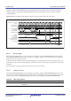
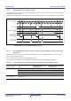
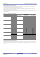
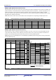
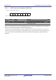
Table Of Contents
- 29. Low-Power Timer (LPT)
- 29.1 Overview
- 29.2 Register Descriptions
- 29.2.1 Low-Power Timer Control Register 1 (LPTCR1)
- 29.2.2 Low-Power Timer Control Register 2 (LPTCR2)
- 29.2.3 Low-Power Timer Control Register 3 (LPTCR3)
- 29.2.4 Low-Power Timer Period Setting Register (LPTPRD)
- 29.2.5 Low-Power Timer Compare Register 0 (LPCMR0)
- 29.2.6 Low-Power Timer Standby Wakeup Enable Register (LPWUCR)
- 29.3 Operation
- 29.4 Wakeup from Software Standby Mode by an Interrupt through the Event Link Controller (ELC)
- 29.5 Usage Notes
- 30. Watchdog Timer (WDTA)
- 30.1 Overview
- 30.2 Register Descriptions
- 30.3 Operation
- 31. Independent Watchdog Timer (IWDTa)
- 31.1 Overview
- 31.2 Register Descriptions
- 31.3 Operation
- 31.3.1 Count Operation in Each Start Mode
- 31.3.2 Control over Writing to the IWDTCR, IWDTRCR, and IWDTCSTPR Registers
- 31.3.3 Refresh Operation
- 31.3.4 Status Flags
- 31.3.5 Reset Output
- 31.3.6 Interrupt Sources
- 31.3.7 Reading the Counter Value
- 31.3.8 Correspondence between Option Function Select Register 0 (OFS0) and IWDT Registers
- 31.4 Link Operation by ELC
- 31.5 Usage Notes
- 32. USB 2.0 Host/Function Module (USBc)
- 32.1 Overview
- 32.2 Register Descriptions
- 32.2.1 System Configuration Control Register (SYSCFG)
- 32.2.2 System Configuration Status Register 0 (SYSSTS0)
- 32.2.3 Device State Control Register 0 (DVSTCTR0)
- 32.2.4 CFIFO Port Register (CFIFO), D0FIFO Port Register (D0FIFO), D1FIFO Port Register (D1FIFO)
- 32.2.5 CFIFO Port Select Register (CFIFOSEL), D0FIFO Port Select Register (D0FIFOSEL), D1FIFO Port Select Register (D1FIFOSEL)
- 32.2.6 CFIFO Port Control Register (CFIFOCTR), D0FIFO Port Control Register (D0FIFOCTR), D1FIFO Port Control Register (D1FIFOCTR)
- 32.2.7 Interrupt Enable Register 0 (INTENB0)
- 32.2.8 Interrupt Enable Register 1 (INTENB1)
- 32.2.9 BRDY Interrupt Enable Register (BRDYENB)
- 32.2.10 NRDY Interrupt Enable Register (NRDYENB)
- 32.2.11 BEMP Interrupt Enable Register (BEMPENB)
- 32.2.12 SOF Output Configuration Register (SOFCFG)
- 32.2.13 Interrupt Status Register 0 (INTSTS0)
- 32.2.14 Interrupt Status Register 1 (INTSTS1)
- 32.2.15 BRDY Interrupt Status Register (BRDYSTS)
- 32.2.16 NRDY Interrupt Status Register (NRDYSTS)
- 32.2.17 BEMP Interrupt Status Register (BEMPSTS)
- 32.2.18 Frame Number Register (FRMNUM)
- 32.2.19 USB Request Type Register (USBREQ)
- 32.2.20 USB Request Value Register (USBVAL)
- 32.2.21 USB Request Index Register (USBINDX)
- 32.2.22 USB Request Length Register (USBLENG)
- 32.2.23 DCP Configuration Register (DCPCFG)
- 32.2.24 DCP Maximum Packet Size Register (DCPMAXP)
- 32.2.25 DCP Control Register (DCPCTR)
- 32.2.26 Pipe Window Select Register (PIPESEL)
- 32.2.27 Pipe Configuration Register (PIPECFG)
- 32.2.28 Pipe Maximum Packet Size Register (PIPEMAXP)
- 32.2.29 Pipe Cycle Control Register (PIPEPERI)
- 32.2.30 Pipe n Control Registers (PIPEnCTR) (n = 1 to 9)
- 32.2.31 Pipe n Transaction Counter Enable Register (PIPEnTRE) (n = 1 to 5)
- 32.2.32 Pipe n Transaction Counter Register (PIPEnTRN) (n = 1 to 5)
- 32.2.33 Device Address n Configuration Register (DEVADDn) (n = 0 to 5)
- 32.2.34 USB Module Control Register (USBMC)
- 32.2.35 BC Control Register 0 (USBBCCTRL0)
- 32.3 Operation
- 32.3.1 System Control
- 32.3.2 Interrupt Sources
- 32.3.3 Interrupt Descriptions
- 32.3.3.1 BRDY Interrupt
- 32.3.3.2 NRDY Interrupt
- 32.3.3.3 BEMP Interrupt
- 32.3.3.4 Device State Transition Interrupt
- 32.3.3.5 Control Transfer Stage Transition Interrupt
- 32.3.3.6 Frame Update Interrupt
- 32.3.3.7 VBUS Interrupt
- 32.3.3.8 Resume Interrupt
- 32.3.3.9 OVRCR Interrupt
- 32.3.3.10 BCHG Interrupt
- 32.3.3.11 DTCH Interrupt
- 32.3.3.12 SACK Interrupt
- 32.3.3.13 SIGN Interrupt
- 32.3.3.14 ATTCH Interrupt
- 32.3.3.15 EOFERR Interrupt
- 32.3.3.16 Portable Device Detection Interrupt
- 32.3.4 Pipe Control
- 32.3.4.1 Pipe Control Register Switching Procedures
- 32.3.4.2 Transfer Types
- 32.3.4.3 Endpoint Number
- 32.3.4.4 Maximum Packet Size Setting
- 32.3.4.5 Transaction Counter (For Pipes 1 to 5 in Reading Direction)
- 32.3.4.6 Response PID
- 32.3.4.7 Data PID Sequence Bit
- 32.3.4.8 Response PID = NAK Function
- 32.3.4.9 Auto Response Mode
- 32.3.4.10 OUT-NAK Mode
- 32.3.4.11 Null Auto Response Mode
- 32.3.5 FIFO Buffer Memory
- 32.3.6 Control Transfers Using DCP
- 32.3.7 Bulk Transfers (Pipes 1 to 5)
- 32.3.8 Interrupt Transfers (Pipes 6 to 9)
- 32.3.9 Isochronous Transfers (Pipes 1 and 2)
- 32.3.10 SOF Interpolation Function
- 32.3.11 Pipe Schedule
- 32.4 Usage Notes
- 32.5 Battery Charging Detection Processing
- 33. Serial Communications Interface (SCIg, SCIh)
- 33.1 Overview
- 33.2 Register Descriptions
- 33.2.1 Receive Shift Register (RSR)
- 33.2.2 Receive Data Register (RDR)
- 33.2.3 Receive Data Register H, L, HL (RDRH, RDRL, RDRHL)
- 33.2.4 Transmit Data Register (TDR)
- 33.2.5 Transmit Data Register H, L, HL (TDRH, TDRL, TDRHL)
- 33.2.6 Transmit Shift Register (TSR)
- 33.2.7 Serial Mode Register (SMR)
- 33.2.8 Serial Control Register (SCR)
- 33.2.9 Serial Status Register (SSR)
- 33.2.10 Smart Card Mode Register (SCMR)
- 33.2.11 Bit Rate Register (BRR)

R01UH0823EJ0110 Rev.1.10 Page 847 of 1852
Nov 30, 2020
RX23W Group 31. Independent Watchdog Timer (IWDTa)
RPES[1:0] Bits (Window End Position Select)
These bits select 75%, 50%, 25% or 0% of the count period for the window end position of the counter. The window end
position should be a value smaller than the window start position (window start position > window end position). If the
window end position is greater than the window start position, only the window start position setting is enabled.
The counter values for the window start and end positions selected by setting the RPSS[1:0] and RPES[1:0] bits change
depending on the TOPS[1:0] bit setting.
Table 31.3 lists the counter values for the window start and end positions corresponding to TOPS[1:0] bit values.
RPSS[1:0] Bits (Window Start Position Select)
These bits select a counter window start position from 100%, 75%, 50%, or 25% of the count period (100% when the
count starts and 0% when the counter underflows). The interval between the window start position and window end
position is the refresh-permitted period and the other periods are refresh-prohibited periods.
Figure 31.2 shows the relationship between of the RPSS[1:0] and RPES[1:0] bit setting and the refresh-permitted and
refresh-prohibited periods.
Figure 31.2 RPSS[1:0] and RPES[1:0] Bit Settings and the Refresh-Permitted Period
Table 31.3 Relationship between Timeout Period and Window Start and End Counter Values
TOPS[1:0] Bits Timeout Period Window Start and End Counter Value
b1 b0 Cycles Counter Value 100% 75% 50% 25%
0 0 128 007Fh 007Fh 005Fh 003Fh 001Fh
0 1 512 01FFh 01FFh 017Fh 00FFh 007Fh
1 0 1024 03FFh 03FFh 02FFh 01FFh 00FFh
1 1 2048 07FFh 07FFh 05FFh 03FFh 01FFh
Window
Start
(%)
End
1
25
0%
Refresh-permitted period
Underflow
100% 75% 50% 25%
100
75
50
Counting
started
RPSS[1:0] Bits
RPES[1:0] Bits
1
Refresh-prohibited period
(%)
1
1
10
0
0
0
1
1
10
0
0
0
1
1
1
10
0
0
0
1
1
1
10
0
0
0
1
1
1
10
0
0
0
0
25
50
75
0
25
50
75
0
25
50
75
0
25
50
75
b13
b9
b12
b8
Note: If window end setting is greater than or equal to window start setting,
the window end setting is set to 0%.