
How-To Guide
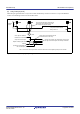
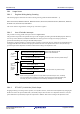
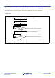
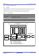
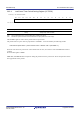
Table Of Contents
- 29. Low-Power Timer (LPT)
- 29.1 Overview
- 29.2 Register Descriptions
- 29.2.1 Low-Power Timer Control Register 1 (LPTCR1)
- 29.2.2 Low-Power Timer Control Register 2 (LPTCR2)
- 29.2.3 Low-Power Timer Control Register 3 (LPTCR3)
- 29.2.4 Low-Power Timer Period Setting Register (LPTPRD)
- 29.2.5 Low-Power Timer Compare Register 0 (LPCMR0)
- 29.2.6 Low-Power Timer Standby Wakeup Enable Register (LPWUCR)
- 29.3 Operation
- 29.4 Wakeup from Software Standby Mode by an Interrupt through the Event Link Controller (ELC)
- 29.5 Usage Notes
- 30. Watchdog Timer (WDTA)
- 30.1 Overview
- 30.2 Register Descriptions
- 30.3 Operation
- 31. Independent Watchdog Timer (IWDTa)
- 31.1 Overview
- 31.2 Register Descriptions
- 31.3 Operation
- 31.3.1 Count Operation in Each Start Mode
- 31.3.2 Control over Writing to the IWDTCR, IWDTRCR, and IWDTCSTPR Registers
- 31.3.3 Refresh Operation
- 31.3.4 Status Flags
- 31.3.5 Reset Output
- 31.3.6 Interrupt Sources
- 31.3.7 Reading the Counter Value
- 31.3.8 Correspondence between Option Function Select Register 0 (OFS0) and IWDT Registers
- 31.4 Link Operation by ELC
- 31.5 Usage Notes
- 32. USB 2.0 Host/Function Module (USBc)
- 32.1 Overview
- 32.2 Register Descriptions
- 32.2.1 System Configuration Control Register (SYSCFG)
- 32.2.2 System Configuration Status Register 0 (SYSSTS0)
- 32.2.3 Device State Control Register 0 (DVSTCTR0)
- 32.2.4 CFIFO Port Register (CFIFO), D0FIFO Port Register (D0FIFO), D1FIFO Port Register (D1FIFO)
- 32.2.5 CFIFO Port Select Register (CFIFOSEL), D0FIFO Port Select Register (D0FIFOSEL), D1FIFO Port Select Register (D1FIFOSEL)
- 32.2.6 CFIFO Port Control Register (CFIFOCTR), D0FIFO Port Control Register (D0FIFOCTR), D1FIFO Port Control Register (D1FIFOCTR)
- 32.2.7 Interrupt Enable Register 0 (INTENB0)
- 32.2.8 Interrupt Enable Register 1 (INTENB1)
- 32.2.9 BRDY Interrupt Enable Register (BRDYENB)
- 32.2.10 NRDY Interrupt Enable Register (NRDYENB)
- 32.2.11 BEMP Interrupt Enable Register (BEMPENB)
- 32.2.12 SOF Output Configuration Register (SOFCFG)
- 32.2.13 Interrupt Status Register 0 (INTSTS0)
- 32.2.14 Interrupt Status Register 1 (INTSTS1)
- 32.2.15 BRDY Interrupt Status Register (BRDYSTS)
- 32.2.16 NRDY Interrupt Status Register (NRDYSTS)
- 32.2.17 BEMP Interrupt Status Register (BEMPSTS)
- 32.2.18 Frame Number Register (FRMNUM)
- 32.2.19 USB Request Type Register (USBREQ)
- 32.2.20 USB Request Value Register (USBVAL)
- 32.2.21 USB Request Index Register (USBINDX)
- 32.2.22 USB Request Length Register (USBLENG)
- 32.2.23 DCP Configuration Register (DCPCFG)
- 32.2.24 DCP Maximum Packet Size Register (DCPMAXP)
- 32.2.25 DCP Control Register (DCPCTR)
- 32.2.26 Pipe Window Select Register (PIPESEL)
- 32.2.27 Pipe Configuration Register (PIPECFG)
- 32.2.28 Pipe Maximum Packet Size Register (PIPEMAXP)
- 32.2.29 Pipe Cycle Control Register (PIPEPERI)
- 32.2.30 Pipe n Control Registers (PIPEnCTR) (n = 1 to 9)
- 32.2.31 Pipe n Transaction Counter Enable Register (PIPEnTRE) (n = 1 to 5)
- 32.2.32 Pipe n Transaction Counter Register (PIPEnTRN) (n = 1 to 5)
- 32.2.33 Device Address n Configuration Register (DEVADDn) (n = 0 to 5)
- 32.2.34 USB Module Control Register (USBMC)
- 32.2.35 BC Control Register 0 (USBBCCTRL0)
- 32.3 Operation
- 32.3.1 System Control
- 32.3.2 Interrupt Sources
- 32.3.3 Interrupt Descriptions
- 32.3.3.1 BRDY Interrupt
- 32.3.3.2 NRDY Interrupt
- 32.3.3.3 BEMP Interrupt
- 32.3.3.4 Device State Transition Interrupt
- 32.3.3.5 Control Transfer Stage Transition Interrupt
- 32.3.3.6 Frame Update Interrupt
- 32.3.3.7 VBUS Interrupt
- 32.3.3.8 Resume Interrupt
- 32.3.3.9 OVRCR Interrupt
- 32.3.3.10 BCHG Interrupt
- 32.3.3.11 DTCH Interrupt
- 32.3.3.12 SACK Interrupt
- 32.3.3.13 SIGN Interrupt
- 32.3.3.14 ATTCH Interrupt
- 32.3.3.15 EOFERR Interrupt
- 32.3.3.16 Portable Device Detection Interrupt
- 32.3.4 Pipe Control
- 32.3.4.1 Pipe Control Register Switching Procedures
- 32.3.4.2 Transfer Types
- 32.3.4.3 Endpoint Number
- 32.3.4.4 Maximum Packet Size Setting
- 32.3.4.5 Transaction Counter (For Pipes 1 to 5 in Reading Direction)
- 32.3.4.6 Response PID
- 32.3.4.7 Data PID Sequence Bit
- 32.3.4.8 Response PID = NAK Function
- 32.3.4.9 Auto Response Mode
- 32.3.4.10 OUT-NAK Mode
- 32.3.4.11 Null Auto Response Mode
- 32.3.5 FIFO Buffer Memory
- 32.3.6 Control Transfers Using DCP
- 32.3.7 Bulk Transfers (Pipes 1 to 5)
- 32.3.8 Interrupt Transfers (Pipes 6 to 9)
- 32.3.9 Isochronous Transfers (Pipes 1 and 2)
- 32.3.10 SOF Interpolation Function
- 32.3.11 Pipe Schedule
- 32.4 Usage Notes
- 32.5 Battery Charging Detection Processing
- 33. Serial Communications Interface (SCIg, SCIh)
- 33.1 Overview
- 33.2 Register Descriptions
- 33.2.1 Receive Shift Register (RSR)
- 33.2.2 Receive Data Register (RDR)
- 33.2.3 Receive Data Register H, L, HL (RDRH, RDRL, RDRHL)
- 33.2.4 Transmit Data Register (TDR)
- 33.2.5 Transmit Data Register H, L, HL (TDRH, TDRL, TDRHL)
- 33.2.6 Transmit Shift Register (TSR)
- 33.2.7 Serial Mode Register (SMR)
- 33.2.8 Serial Control Register (SCR)
- 33.2.9 Serial Status Register (SSR)
- 33.2.10 Smart Card Mode Register (SCMR)
- 33.2.11 Bit Rate Register (BRR)

R01UH0823EJ0110 Rev.1.10 Page 816 of 1852
Nov 30, 2020
RX23W Group 29. Low-Power Timer (LPT)
29.2 Register Descriptions
29.2.1 Low-Power Timer Control Register 1 (LPTCR1)
Note: Set the PRCR.PRC2 bit to 1 (write enabled) before rewriting this register.
Note 1. Rewrite these bits while the LPTCR2.LPCNTSTP bit is 1 (supply of clock to the low-power timer is stopped).
Note 2. Satisfy that the frequency of the system clock (ICLK) and peripheral module clock (PCLKB) ≥ 4 × (the frequency of the clock
source).
Note 3. A clock generated by the IWDT-dedicated on-chip oscillator (IWDTCLK) is supplied to the low-power timer. When modifying this
bit, make sure that the IWDT-dedicated on-chip oscillator is oscillating stably.
When the IWDTCLK is used as the clock source for the low-power timer, set the OFS0.IWDTSLCSTP bit to 0 (counting stop is
disabled) in IWDT auto-start mode operation, and set the IWDTCSTPR.SLCSTP bit to 0 (count stop is disabled) in other modes.
Without this setting, the IWDT-dedicated on-chip oscillator is stopped in software standby mode.
Note 4. Rewrite this bit while the LPTCR3.LPCNTEN bit is 0 (low-power timer counter stops).
The LPTCR1 register is used to control the low-power timer.
LPCNTCKSEL Bit (Clock Source Select)
This bit is used to select the sub-clock or IWDT-dedicated clock as the clock source for the low-power timer.
LPCMRE0 Bit (Compare Match 0 Enable)
This bit enables or disables low-power timer compare match 0.
When the low-power timer is put into operation and the MCU makes a transition to software standby mode while this bit
and the LPWUCR.LPWKUPEN bit are set to 1 (wakeup from software standby mode using low-power timer is enabled),
the MCU returns from software standby mode to normal operating mode through the event link controller (ELC) when
the value of the low-power timer counter matches the value of the LPCMR0 register.
Settings for the interrupt and ELC are necessary to use a compare match 0 as a trigger source to return from software
standby mode.
Refer to
section 20, Event Link Controller (ELC) for details on the ELC settings, and refer to section 15, Interrupt
Controller (ICUb)
for details on the interrupt settings.
Address(es): LPT.LPTCR1 0008 00B0h
b7 b6 b5 b4 b3 b2 b1 b0
—
LPCMR
E0
—
LPCNT
CKSEL
— LPCNTPSSEL[2:0]
Value after reset:
00000001
Bit Symbol Bit Name Description R/W
b2 to b0 LPCNTPSSEL[2:0] Clock Division Ratio Select*
1
b2 b0
0 0 1: Divided by 2
0 1 0: Divided by 4
0 1 1: Divided by 8
1 0 0: Divided by 16
1 0 1: Divided by 32
Settings other than above are prohibited.
R/W
b3 — Reserved This bit is read as 0. The write value should be 0. R/W
b4 LPCNTCKSEL Clock Source Select*
1,
*
2
0: Sub-clock
1: IWDT-dedicated clock (IWDTCLK)*
3
R/W
b5 — Reserved This bit is read as 0. The write value should be 0. R/W
b6 LPCMRE0 Compare Match 0 Enable*
4
0: Compare match 0 is disabled
1: Compare match 0 is enabled
R/W
b7 — Reserved This bit is read as 0. The write value should be 0. R/W