
How-To Guide
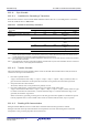
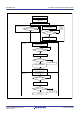
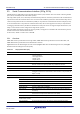
Table Of Contents
- 29. Low-Power Timer (LPT)
- 29.1 Overview
- 29.2 Register Descriptions
- 29.2.1 Low-Power Timer Control Register 1 (LPTCR1)
- 29.2.2 Low-Power Timer Control Register 2 (LPTCR2)
- 29.2.3 Low-Power Timer Control Register 3 (LPTCR3)
- 29.2.4 Low-Power Timer Period Setting Register (LPTPRD)
- 29.2.5 Low-Power Timer Compare Register 0 (LPCMR0)
- 29.2.6 Low-Power Timer Standby Wakeup Enable Register (LPWUCR)
- 29.3 Operation
- 29.4 Wakeup from Software Standby Mode by an Interrupt through the Event Link Controller (ELC)
- 29.5 Usage Notes
- 30. Watchdog Timer (WDTA)
- 30.1 Overview
- 30.2 Register Descriptions
- 30.3 Operation
- 31. Independent Watchdog Timer (IWDTa)
- 31.1 Overview
- 31.2 Register Descriptions
- 31.3 Operation
- 31.3.1 Count Operation in Each Start Mode
- 31.3.2 Control over Writing to the IWDTCR, IWDTRCR, and IWDTCSTPR Registers
- 31.3.3 Refresh Operation
- 31.3.4 Status Flags
- 31.3.5 Reset Output
- 31.3.6 Interrupt Sources
- 31.3.7 Reading the Counter Value
- 31.3.8 Correspondence between Option Function Select Register 0 (OFS0) and IWDT Registers
- 31.4 Link Operation by ELC
- 31.5 Usage Notes
- 32. USB 2.0 Host/Function Module (USBc)
- 32.1 Overview
- 32.2 Register Descriptions
- 32.2.1 System Configuration Control Register (SYSCFG)
- 32.2.2 System Configuration Status Register 0 (SYSSTS0)
- 32.2.3 Device State Control Register 0 (DVSTCTR0)
- 32.2.4 CFIFO Port Register (CFIFO), D0FIFO Port Register (D0FIFO), D1FIFO Port Register (D1FIFO)
- 32.2.5 CFIFO Port Select Register (CFIFOSEL), D0FIFO Port Select Register (D0FIFOSEL), D1FIFO Port Select Register (D1FIFOSEL)
- 32.2.6 CFIFO Port Control Register (CFIFOCTR), D0FIFO Port Control Register (D0FIFOCTR), D1FIFO Port Control Register (D1FIFOCTR)
- 32.2.7 Interrupt Enable Register 0 (INTENB0)
- 32.2.8 Interrupt Enable Register 1 (INTENB1)
- 32.2.9 BRDY Interrupt Enable Register (BRDYENB)
- 32.2.10 NRDY Interrupt Enable Register (NRDYENB)
- 32.2.11 BEMP Interrupt Enable Register (BEMPENB)
- 32.2.12 SOF Output Configuration Register (SOFCFG)
- 32.2.13 Interrupt Status Register 0 (INTSTS0)
- 32.2.14 Interrupt Status Register 1 (INTSTS1)
- 32.2.15 BRDY Interrupt Status Register (BRDYSTS)
- 32.2.16 NRDY Interrupt Status Register (NRDYSTS)
- 32.2.17 BEMP Interrupt Status Register (BEMPSTS)
- 32.2.18 Frame Number Register (FRMNUM)
- 32.2.19 USB Request Type Register (USBREQ)
- 32.2.20 USB Request Value Register (USBVAL)
- 32.2.21 USB Request Index Register (USBINDX)
- 32.2.22 USB Request Length Register (USBLENG)
- 32.2.23 DCP Configuration Register (DCPCFG)
- 32.2.24 DCP Maximum Packet Size Register (DCPMAXP)
- 32.2.25 DCP Control Register (DCPCTR)
- 32.2.26 Pipe Window Select Register (PIPESEL)
- 32.2.27 Pipe Configuration Register (PIPECFG)
- 32.2.28 Pipe Maximum Packet Size Register (PIPEMAXP)
- 32.2.29 Pipe Cycle Control Register (PIPEPERI)
- 32.2.30 Pipe n Control Registers (PIPEnCTR) (n = 1 to 9)
- 32.2.31 Pipe n Transaction Counter Enable Register (PIPEnTRE) (n = 1 to 5)
- 32.2.32 Pipe n Transaction Counter Register (PIPEnTRN) (n = 1 to 5)
- 32.2.33 Device Address n Configuration Register (DEVADDn) (n = 0 to 5)
- 32.2.34 USB Module Control Register (USBMC)
- 32.2.35 BC Control Register 0 (USBBCCTRL0)
- 32.3 Operation
- 32.3.1 System Control
- 32.3.2 Interrupt Sources
- 32.3.3 Interrupt Descriptions
- 32.3.3.1 BRDY Interrupt
- 32.3.3.2 NRDY Interrupt
- 32.3.3.3 BEMP Interrupt
- 32.3.3.4 Device State Transition Interrupt
- 32.3.3.5 Control Transfer Stage Transition Interrupt
- 32.3.3.6 Frame Update Interrupt
- 32.3.3.7 VBUS Interrupt
- 32.3.3.8 Resume Interrupt
- 32.3.3.9 OVRCR Interrupt
- 32.3.3.10 BCHG Interrupt
- 32.3.3.11 DTCH Interrupt
- 32.3.3.12 SACK Interrupt
- 32.3.3.13 SIGN Interrupt
- 32.3.3.14 ATTCH Interrupt
- 32.3.3.15 EOFERR Interrupt
- 32.3.3.16 Portable Device Detection Interrupt
- 32.3.4 Pipe Control
- 32.3.4.1 Pipe Control Register Switching Procedures
- 32.3.4.2 Transfer Types
- 32.3.4.3 Endpoint Number
- 32.3.4.4 Maximum Packet Size Setting
- 32.3.4.5 Transaction Counter (For Pipes 1 to 5 in Reading Direction)
- 32.3.4.6 Response PID
- 32.3.4.7 Data PID Sequence Bit
- 32.3.4.8 Response PID = NAK Function
- 32.3.4.9 Auto Response Mode
- 32.3.4.10 OUT-NAK Mode
- 32.3.4.11 Null Auto Response Mode
- 32.3.5 FIFO Buffer Memory
- 32.3.6 Control Transfers Using DCP
- 32.3.7 Bulk Transfers (Pipes 1 to 5)
- 32.3.8 Interrupt Transfers (Pipes 6 to 9)
- 32.3.9 Isochronous Transfers (Pipes 1 and 2)
- 32.3.10 SOF Interpolation Function
- 32.3.11 Pipe Schedule
- 32.4 Usage Notes
- 32.5 Battery Charging Detection Processing
- 33. Serial Communications Interface (SCIg, SCIh)
- 33.1 Overview
- 33.2 Register Descriptions
- 33.2.1 Receive Shift Register (RSR)
- 33.2.2 Receive Data Register (RDR)
- 33.2.3 Receive Data Register H, L, HL (RDRH, RDRL, RDRHL)
- 33.2.4 Transmit Data Register (TDR)
- 33.2.5 Transmit Data Register H, L, HL (TDRH, TDRL, TDRHL)
- 33.2.6 Transmit Shift Register (TSR)
- 33.2.7 Serial Mode Register (SMR)
- 33.2.8 Serial Control Register (SCR)
- 33.2.9 Serial Status Register (SSR)
- 33.2.10 Smart Card Mode Register (SCMR)
- 33.2.11 Bit Rate Register (BRR)

R01UH0823EJ0110 Rev.1.10 Page 967 of 1852
Nov 30, 2020
RX23W Group 32. USB 2.0 Host/Function Module (USBc)
Figure 32.21 Process Flow for Operating as Charging Downstream Port (Steps (1) to (4))
D-Line Drive
Control
Portable Device
Detection
Processing
Drive VBUS
PD detection interrupt?
(PDDETINT)
Connection detected?
(D+ pull-up detected?)
Target is normal peripheral
device
Set VDMSRCE0 bit to 1
PDDETSTS0 bit = 1?
PD detection interrupt?
(PDDETINT)
PDDETSTS0 bit = 0?
Target is normal portable device
Connection detected?
(D+ pull-up detected?)
Set VDMSRCE0 bit to 0
PD detection interrupt enabled
(PDDETINTE0 = 1)
Repeat reading several times
to perform debouncing.
Repeat reading
several times to
perform debouncing.
PD detection circuit enabled
(IDPSINKE0 = 1)
No
Yes
No
Yes
No
Yes
No
Yes
Yes
No
No
Yes
If SUSP = 0, use BCHG interrupt and
LNST[1:0] for verification.
If SUSP = 1, use ATTCH interrupt for
verification.
If SUSP = 0, use BCHG interrupt and
LNST[1:0] for verification.
If SUSP = 1, use ATTCH interrupt for
verification.