
How-To Guide
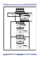
Table Of Contents
- 29. Low-Power Timer (LPT)
- 29.1 Overview
- 29.2 Register Descriptions
- 29.2.1 Low-Power Timer Control Register 1 (LPTCR1)
- 29.2.2 Low-Power Timer Control Register 2 (LPTCR2)
- 29.2.3 Low-Power Timer Control Register 3 (LPTCR3)
- 29.2.4 Low-Power Timer Period Setting Register (LPTPRD)
- 29.2.5 Low-Power Timer Compare Register 0 (LPCMR0)
- 29.2.6 Low-Power Timer Standby Wakeup Enable Register (LPWUCR)
- 29.3 Operation
- 29.4 Wakeup from Software Standby Mode by an Interrupt through the Event Link Controller (ELC)
- 29.5 Usage Notes
- 30. Watchdog Timer (WDTA)
- 30.1 Overview
- 30.2 Register Descriptions
- 30.3 Operation
- 31. Independent Watchdog Timer (IWDTa)
- 31.1 Overview
- 31.2 Register Descriptions
- 31.3 Operation
- 31.3.1 Count Operation in Each Start Mode
- 31.3.2 Control over Writing to the IWDTCR, IWDTRCR, and IWDTCSTPR Registers
- 31.3.3 Refresh Operation
- 31.3.4 Status Flags
- 31.3.5 Reset Output
- 31.3.6 Interrupt Sources
- 31.3.7 Reading the Counter Value
- 31.3.8 Correspondence between Option Function Select Register 0 (OFS0) and IWDT Registers
- 31.4 Link Operation by ELC
- 31.5 Usage Notes
- 32. USB 2.0 Host/Function Module (USBc)
- 32.1 Overview
- 32.2 Register Descriptions
- 32.2.1 System Configuration Control Register (SYSCFG)
- 32.2.2 System Configuration Status Register 0 (SYSSTS0)
- 32.2.3 Device State Control Register 0 (DVSTCTR0)
- 32.2.4 CFIFO Port Register (CFIFO), D0FIFO Port Register (D0FIFO), D1FIFO Port Register (D1FIFO)
- 32.2.5 CFIFO Port Select Register (CFIFOSEL), D0FIFO Port Select Register (D0FIFOSEL), D1FIFO Port Select Register (D1FIFOSEL)
- 32.2.6 CFIFO Port Control Register (CFIFOCTR), D0FIFO Port Control Register (D0FIFOCTR), D1FIFO Port Control Register (D1FIFOCTR)
- 32.2.7 Interrupt Enable Register 0 (INTENB0)
- 32.2.8 Interrupt Enable Register 1 (INTENB1)
- 32.2.9 BRDY Interrupt Enable Register (BRDYENB)
- 32.2.10 NRDY Interrupt Enable Register (NRDYENB)
- 32.2.11 BEMP Interrupt Enable Register (BEMPENB)
- 32.2.12 SOF Output Configuration Register (SOFCFG)
- 32.2.13 Interrupt Status Register 0 (INTSTS0)
- 32.2.14 Interrupt Status Register 1 (INTSTS1)
- 32.2.15 BRDY Interrupt Status Register (BRDYSTS)
- 32.2.16 NRDY Interrupt Status Register (NRDYSTS)
- 32.2.17 BEMP Interrupt Status Register (BEMPSTS)
- 32.2.18 Frame Number Register (FRMNUM)
- 32.2.19 USB Request Type Register (USBREQ)
- 32.2.20 USB Request Value Register (USBVAL)
- 32.2.21 USB Request Index Register (USBINDX)
- 32.2.22 USB Request Length Register (USBLENG)
- 32.2.23 DCP Configuration Register (DCPCFG)
- 32.2.24 DCP Maximum Packet Size Register (DCPMAXP)
- 32.2.25 DCP Control Register (DCPCTR)
- 32.2.26 Pipe Window Select Register (PIPESEL)
- 32.2.27 Pipe Configuration Register (PIPECFG)
- 32.2.28 Pipe Maximum Packet Size Register (PIPEMAXP)
- 32.2.29 Pipe Cycle Control Register (PIPEPERI)
- 32.2.30 Pipe n Control Registers (PIPEnCTR) (n = 1 to 9)
- 32.2.31 Pipe n Transaction Counter Enable Register (PIPEnTRE) (n = 1 to 5)
- 32.2.32 Pipe n Transaction Counter Register (PIPEnTRN) (n = 1 to 5)
- 32.2.33 Device Address n Configuration Register (DEVADDn) (n = 0 to 5)
- 32.2.34 USB Module Control Register (USBMC)
- 32.2.35 BC Control Register 0 (USBBCCTRL0)
- 32.3 Operation
- 32.3.1 System Control
- 32.3.2 Interrupt Sources
- 32.3.3 Interrupt Descriptions
- 32.3.3.1 BRDY Interrupt
- 32.3.3.2 NRDY Interrupt
- 32.3.3.3 BEMP Interrupt
- 32.3.3.4 Device State Transition Interrupt
- 32.3.3.5 Control Transfer Stage Transition Interrupt
- 32.3.3.6 Frame Update Interrupt
- 32.3.3.7 VBUS Interrupt
- 32.3.3.8 Resume Interrupt
- 32.3.3.9 OVRCR Interrupt
- 32.3.3.10 BCHG Interrupt
- 32.3.3.11 DTCH Interrupt
- 32.3.3.12 SACK Interrupt
- 32.3.3.13 SIGN Interrupt
- 32.3.3.14 ATTCH Interrupt
- 32.3.3.15 EOFERR Interrupt
- 32.3.3.16 Portable Device Detection Interrupt
- 32.3.4 Pipe Control
- 32.3.4.1 Pipe Control Register Switching Procedures
- 32.3.4.2 Transfer Types
- 32.3.4.3 Endpoint Number
- 32.3.4.4 Maximum Packet Size Setting
- 32.3.4.5 Transaction Counter (For Pipes 1 to 5 in Reading Direction)
- 32.3.4.6 Response PID
- 32.3.4.7 Data PID Sequence Bit
- 32.3.4.8 Response PID = NAK Function
- 32.3.4.9 Auto Response Mode
- 32.3.4.10 OUT-NAK Mode
- 32.3.4.11 Null Auto Response Mode
- 32.3.5 FIFO Buffer Memory
- 32.3.6 Control Transfers Using DCP
- 32.3.7 Bulk Transfers (Pipes 1 to 5)
- 32.3.8 Interrupt Transfers (Pipes 6 to 9)
- 32.3.9 Isochronous Transfers (Pipes 1 and 2)
- 32.3.10 SOF Interpolation Function
- 32.3.11 Pipe Schedule
- 32.4 Usage Notes
- 32.5 Battery Charging Detection Processing
- 33. Serial Communications Interface (SCIg, SCIh)
- 33.1 Overview
- 33.2 Register Descriptions
- 33.2.1 Receive Shift Register (RSR)
- 33.2.2 Receive Data Register (RDR)
- 33.2.3 Receive Data Register H, L, HL (RDRH, RDRL, RDRHL)
- 33.2.4 Transmit Data Register (TDR)
- 33.2.5 Transmit Data Register H, L, HL (TDRH, TDRL, TDRHL)
- 33.2.6 Transmit Shift Register (TSR)
- 33.2.7 Serial Mode Register (SMR)
- 33.2.8 Serial Control Register (SCR)
- 33.2.9 Serial Status Register (SSR)
- 33.2.10 Smart Card Mode Register (SCMR)
- 33.2.11 Bit Rate Register (BRR)

R01UH0823EJ0110 Rev.1.10 Page 961 of 1852
Nov 30, 2020
RX23W Group 32. USB 2.0 Host/Function Module (USBc)
32.3.10 SOF Interpolation Function
When the function controller is selected and if data could not be received at intervals of 1 ms because an SOF packet was
corrupted or missing, the USB interpolates the SOF. The SOF interpolation operation begins when the USBE and SCKE
bits in the SYSCFG register have been set to 1 and an SOF packet is received. The interpolation function is initialized
under the following conditions.
• MCU reset
• USB bus reset
• Suspended state detected
The SOF interpolation operates as follows.
• The interpolation function is not activated until an SOF packet is received.
• After the first SOF packet is received, interpolation is carried out by counting 1 ms with an internal clock of
48 MHz.
• After the second and subsequent SOF packets are received, interpolation is carried out at the previous reception
interval.
• Interpolation is not carried out in the suspended state or while a USB bus reset is being received.
The USB supports the following functions based on the SOF packet reception. These functions also operate normally
with SOF interpolation, if the SOF packet was missing.
• Updating of the frame number
• SOFR interrupt timing
• Isochronous transfer interval count
If an SOF packet is missing, the FRMNUM.FRNM[10:0] flags are not updated.