
How-To Guide
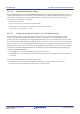
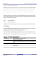
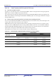
Table Of Contents
- 29. Low-Power Timer (LPT)
- 29.1 Overview
- 29.2 Register Descriptions
- 29.2.1 Low-Power Timer Control Register 1 (LPTCR1)
- 29.2.2 Low-Power Timer Control Register 2 (LPTCR2)
- 29.2.3 Low-Power Timer Control Register 3 (LPTCR3)
- 29.2.4 Low-Power Timer Period Setting Register (LPTPRD)
- 29.2.5 Low-Power Timer Compare Register 0 (LPCMR0)
- 29.2.6 Low-Power Timer Standby Wakeup Enable Register (LPWUCR)
- 29.3 Operation
- 29.4 Wakeup from Software Standby Mode by an Interrupt through the Event Link Controller (ELC)
- 29.5 Usage Notes
- 30. Watchdog Timer (WDTA)
- 30.1 Overview
- 30.2 Register Descriptions
- 30.3 Operation
- 31. Independent Watchdog Timer (IWDTa)
- 31.1 Overview
- 31.2 Register Descriptions
- 31.3 Operation
- 31.3.1 Count Operation in Each Start Mode
- 31.3.2 Control over Writing to the IWDTCR, IWDTRCR, and IWDTCSTPR Registers
- 31.3.3 Refresh Operation
- 31.3.4 Status Flags
- 31.3.5 Reset Output
- 31.3.6 Interrupt Sources
- 31.3.7 Reading the Counter Value
- 31.3.8 Correspondence between Option Function Select Register 0 (OFS0) and IWDT Registers
- 31.4 Link Operation by ELC
- 31.5 Usage Notes
- 32. USB 2.0 Host/Function Module (USBc)
- 32.1 Overview
- 32.2 Register Descriptions
- 32.2.1 System Configuration Control Register (SYSCFG)
- 32.2.2 System Configuration Status Register 0 (SYSSTS0)
- 32.2.3 Device State Control Register 0 (DVSTCTR0)
- 32.2.4 CFIFO Port Register (CFIFO), D0FIFO Port Register (D0FIFO), D1FIFO Port Register (D1FIFO)
- 32.2.5 CFIFO Port Select Register (CFIFOSEL), D0FIFO Port Select Register (D0FIFOSEL), D1FIFO Port Select Register (D1FIFOSEL)
- 32.2.6 CFIFO Port Control Register (CFIFOCTR), D0FIFO Port Control Register (D0FIFOCTR), D1FIFO Port Control Register (D1FIFOCTR)
- 32.2.7 Interrupt Enable Register 0 (INTENB0)
- 32.2.8 Interrupt Enable Register 1 (INTENB1)
- 32.2.9 BRDY Interrupt Enable Register (BRDYENB)
- 32.2.10 NRDY Interrupt Enable Register (NRDYENB)
- 32.2.11 BEMP Interrupt Enable Register (BEMPENB)
- 32.2.12 SOF Output Configuration Register (SOFCFG)
- 32.2.13 Interrupt Status Register 0 (INTSTS0)
- 32.2.14 Interrupt Status Register 1 (INTSTS1)
- 32.2.15 BRDY Interrupt Status Register (BRDYSTS)
- 32.2.16 NRDY Interrupt Status Register (NRDYSTS)
- 32.2.17 BEMP Interrupt Status Register (BEMPSTS)
- 32.2.18 Frame Number Register (FRMNUM)
- 32.2.19 USB Request Type Register (USBREQ)
- 32.2.20 USB Request Value Register (USBVAL)
- 32.2.21 USB Request Index Register (USBINDX)
- 32.2.22 USB Request Length Register (USBLENG)
- 32.2.23 DCP Configuration Register (DCPCFG)
- 32.2.24 DCP Maximum Packet Size Register (DCPMAXP)
- 32.2.25 DCP Control Register (DCPCTR)
- 32.2.26 Pipe Window Select Register (PIPESEL)
- 32.2.27 Pipe Configuration Register (PIPECFG)
- 32.2.28 Pipe Maximum Packet Size Register (PIPEMAXP)
- 32.2.29 Pipe Cycle Control Register (PIPEPERI)
- 32.2.30 Pipe n Control Registers (PIPEnCTR) (n = 1 to 9)
- 32.2.31 Pipe n Transaction Counter Enable Register (PIPEnTRE) (n = 1 to 5)
- 32.2.32 Pipe n Transaction Counter Register (PIPEnTRN) (n = 1 to 5)
- 32.2.33 Device Address n Configuration Register (DEVADDn) (n = 0 to 5)
- 32.2.34 USB Module Control Register (USBMC)
- 32.2.35 BC Control Register 0 (USBBCCTRL0)
- 32.3 Operation
- 32.3.1 System Control
- 32.3.2 Interrupt Sources
- 32.3.3 Interrupt Descriptions
- 32.3.3.1 BRDY Interrupt
- 32.3.3.2 NRDY Interrupt
- 32.3.3.3 BEMP Interrupt
- 32.3.3.4 Device State Transition Interrupt
- 32.3.3.5 Control Transfer Stage Transition Interrupt
- 32.3.3.6 Frame Update Interrupt
- 32.3.3.7 VBUS Interrupt
- 32.3.3.8 Resume Interrupt
- 32.3.3.9 OVRCR Interrupt
- 32.3.3.10 BCHG Interrupt
- 32.3.3.11 DTCH Interrupt
- 32.3.3.12 SACK Interrupt
- 32.3.3.13 SIGN Interrupt
- 32.3.3.14 ATTCH Interrupt
- 32.3.3.15 EOFERR Interrupt
- 32.3.3.16 Portable Device Detection Interrupt
- 32.3.4 Pipe Control
- 32.3.4.1 Pipe Control Register Switching Procedures
- 32.3.4.2 Transfer Types
- 32.3.4.3 Endpoint Number
- 32.3.4.4 Maximum Packet Size Setting
- 32.3.4.5 Transaction Counter (For Pipes 1 to 5 in Reading Direction)
- 32.3.4.6 Response PID
- 32.3.4.7 Data PID Sequence Bit
- 32.3.4.8 Response PID = NAK Function
- 32.3.4.9 Auto Response Mode
- 32.3.4.10 OUT-NAK Mode
- 32.3.4.11 Null Auto Response Mode
- 32.3.5 FIFO Buffer Memory
- 32.3.6 Control Transfers Using DCP
- 32.3.7 Bulk Transfers (Pipes 1 to 5)
- 32.3.8 Interrupt Transfers (Pipes 6 to 9)
- 32.3.9 Isochronous Transfers (Pipes 1 and 2)
- 32.3.10 SOF Interpolation Function
- 32.3.11 Pipe Schedule
- 32.4 Usage Notes
- 32.5 Battery Charging Detection Processing
- 33. Serial Communications Interface (SCIg, SCIh)
- 33.1 Overview
- 33.2 Register Descriptions
- 33.2.1 Receive Shift Register (RSR)
- 33.2.2 Receive Data Register (RDR)
- 33.2.3 Receive Data Register H, L, HL (RDRH, RDRL, RDRHL)
- 33.2.4 Transmit Data Register (TDR)
- 33.2.5 Transmit Data Register H, L, HL (TDRH, TDRL, TDRHL)
- 33.2.6 Transmit Shift Register (TSR)
- 33.2.7 Serial Mode Register (SMR)
- 33.2.8 Serial Control Register (SCR)
- 33.2.9 Serial Status Register (SSR)
- 33.2.10 Smart Card Mode Register (SCMR)
- 33.2.11 Bit Rate Register (BRR)

R01UH0823EJ0110 Rev.1.10 Page 949 of 1852
Nov 30, 2020
RX23W Group 32. USB 2.0 Host/Function Module (USBc)
32.3.5.4 DMA Transfers (D0FIFO and D1FIFO Ports)
(1) Overview of DMA Transfers
For pipes 1 to 9, the FIFO port can be accessed using the DMAC. When accessing the buffer for the pipe targeted for
DMA transfer is enabled, a DMA transfer request is issued.
The unit of transfer to the FIFO port should be selected using the DnFIFOSEL.MBW bit and the pipe targeted for the
DMA transfer should be selected using the DnFIFOSEL.CURPIPE[3:0] bits. The selected pipe should not be changed
during the DMA transfer.
(2) DnFIFO Auto Clear Mode (D0FIFO and D1FIFO Port Reading Direction)
If 1 is set in the DnFIFOSEL.DCLRM bit, the USB automatically clears the buffer memory of the selected pipe when
reading of data from the buffer memory has been completed.
Table 32.21 shows the packet reception and buffer memory clearing processing by software for each of the various
settings. As shown in
Table 32.21, the buffer clearing conditions depend on the value set in the PIPECFG.BFRE bit.
Using the DnFIFOSEL.DCLRM bit eliminates the need for the buffer to be cleared by software in any situation that
requires buffer clearing. This enables DMA transfers without involving software.
The DnFIFO auto clear mode can be set only in the buffer memory reading direction.
Table 32.21 Packet Reception and Buffer Memory Clearing Processing by Software
Buffer Status
When Packet is Received
Register Setting
DCLRM = 0 DCLRM = 1
BFRE = 0 BFRE = 1 BFRE = 0 BFRE = 1
Buffer full Clearing is not
necessary
Clearing is not
necessary
Clearing is not
necessary
Clearing is not
necessary
Zero-length packet reception Clearing is necessary Clearing is necessary Clearing is not
necessary
Clearing is not
necessary
Normal short packet reception Clearing is not
necessary
Clearing is necessary Clearing is not
necessary
Clearing is not
necessary
Transaction count end Clearing is not
necessary
Clearing is necessary Clearing is not
necessary
Clearing is not
necessary