RX23W Group 28.3 28. Realtime Clock (RTCe) Operation 28.3.1 Outline of Initial Settings of Registers after Power On After the power is turned on, the initial settings for the clock setting, count mode setting, time error adjustment, time setting, alarm, interrupt, and time capture control register should be performed.
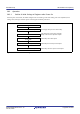
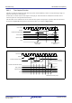
RX23W Group 28.3.2 28. Realtime Clock (RTCe) Clock and Count Mode Setting Procedure Figure 28.3 shows how to set the clock and the count mode. Set the sub-clock oscillator Set the RCR3 register Supply 6 clocks of the count source Set the START bit to 0 No START = 0? Wait for the RCR2.START bit to become 0 Yes Select count mode No CNTMD = the set value? RCR2.CNTMD bit setting*1 Wait until the RCR2.
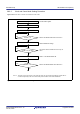
RX23W Group 28.3.3 28. Realtime Clock (RTCe) Setting the Time Figure 28.4 shows how to set the time. Set the START bit to 0 No Write 0 to the RCR2.START bit Wait for the RCR2.START bit to become 0 START = 0? Yes Write 1 to the RCR2.RESET bit*1 Execute an RTC software reset No Wait for the RCR2.
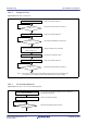
RX23W Group 28.3.5 28. Realtime Clock (RTCe) Reading 64-Hz Counter and Time Figure 28.6 shows how to read the 64-Hz counter and time. (a) To read the time without using interrupt Disable a carry interrupt request on ICU side Write 0 to the ICU.IERm.IENj bit corresponding to the CUP interrupt Enable a carry interrupt request on RTC side Write 1 to the RCR1.CIE bit Clear the interrupt status flag Write 0 to the ICU.IRn.
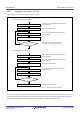
RX23W Group 28.3.6 28. Realtime Clock (RTCe) Alarm Function Figure 28.7 shows how to use the alarm function. Confirm that the RCR2.START bit is 1 (the clock is operating) Check if the clock is operationg Disable an alarm interrupt request on ICU side Set the alarm time and enable the alarm at the same time or later Set the time of the alarm Enable an alarm interrupt request on RTC side and set an interrupt generation period AIE = 1 and PES[3:0] = the set value? Write 0 to the ICU.IERm.
RX23W Group 28.3.7 28. Realtime Clock (RTCe) Procedure for Disabling Alarm Interrupt Figure 28.8 shows the procedure for disabling the enabled alarm interrupt request. An alarm interrupt is enabled Start while the RCR1.AIE bit is 1 Disable an alarm interrupt request on ICU side Write 0 to the ICU.IERm.IENj bit corresponding to the ALM interrupt Disable an alarm interrupt request of RTC side Write 0 to the RCR1.AIE bit No AIE bit = 0? Wait for the RCR1.
RX23W Group 28. Realtime Clock (RTCe) [Example 2] Sub-clock running at 32.766 kHz Adjustment procedure: When the sub-clock is running at 32.766 kHz, 1 second elapses every 32,766 clock cycles. The RTC is meant to run at 32,768 clock cycles, so the clock runs slow by two clock cycles every second. The time on the clock is slow by 20 clock cycles every 10 seconds, so adjustment can take the form of setting the clock forward by 20 cycles every 10 seconds. Register settings: (when RCR2.CNTMD = 0) • RCR2.
RX23W Group 28.3.8.3 28. Realtime Clock (RTCe) Procedure for Changing the Mode of Adjustment When changing the mode of adjustment, change the value of the AADJE bit in RCR2 after setting the RADJ.PMADJ[1:0] bits to 00b (adjustment is not performed). Changing from adjustment by software to automatic adjustment: (1) Set the RADJ.PMADJ[1:0] bits to 00b (adjustment is not performed). (2) Set the RCR2.AADJE bit to 1 (automatic adjustment is enabled). (3) Use the RCR2.
RX23W Group 28.3.9 28. Realtime Clock (RTCe) Time Capture Function The RTC is capable of storing the month, date, hour, minute and second/binary counters 3 to 0 by detecting an edge of a signal on a time capture event input pin. A noise filter can also be used on a time capture event input pin. If the noise filter is enabled, the TCST bit is set to 1 when the input level on the pin matches three times. The noise filter can be switched on or off for each of the time capture event input pins.
RX23W Group 28.4 28. Realtime Clock (RTCe) Interrupt Sources There are three interrupt sources in the realtime clock. Table 28.3 lists interrupt sources for the RTC. Table 28.3 RTC Interrupt Sources Name Interrupt Sources ALM Alarm interrupt PRD Periodic interrupt CUP Carry interrupt (1) Alarm interrupt (ALM) This interrupt is generated according to the result of comparison between the alarm registers and realtime clock counters (for details, refer to section 28.3.6, Alarm Function).
RX23W Group (3) 28. Realtime Clock (RTCe) Carry interrupt (CUP) This interrupt is generated when a carry to the second counter/binary counter 0 occurred or a carry to the R64CNT counter occurred during read access to the 64-Hz counter.
RX23W Group 28.5 28. Realtime Clock (RTCe) Event Link Output The RTC outputs the following event signals for the event link controller (ELC), and these can be used to initiate operations by other modules selected in advance. (1) Periodic event output The periodic event signal is output at the interval selected from among 1/256, 1/128, 1/64, 1/32, 1/16, 1/8, 1/4, 1/2, 1, and 2 seconds by the setting of the RCR1.PES[3:0] bits.
RX23W Group 28.6 28. Realtime Clock (RTCe) Usage Notes 28.6.1 Register Writing during Counting The following registers should not be written to during counting (while the RCR2.START bit = 1). RSECCNT/BCNT0, RMINCNT/BCNT1, RHRCNT/BCNT2, RDAYCNT, RWKCNT/BCNT3, RMONCNT, RYRCNT, RCR1.RTCOS, RCR2.RTCOE, RCR2.HR24 The counter must be stopped before writing to any of the above registers. 28.6.2 Use of Periodic Interrupts The procedure for using periodic interrupts is shown in Figure 28.13.
RX23W Group 28.6.4 28. Realtime Clock (RTCe) Transitions to Low Power Consumption Modes after Setting Registers A transition to a low power consumption state (software standby mode, or battery backup) during writing to or updating of an RTC register might destroy the register’s value. After setting a register, confirm that the setting is in place before initiating a transition to a low power consumption state. 28.6.
RX23W Group 28.6.7 28. Realtime Clock (RTCe) Initialization Procedure When the Realtime Clock is Not to be Used Registers in the RTC are not initialized by a reset. Accordingly, depending on the initial state, the generation of an unintentional interrupt request or operation of the counter may lead to increased power consumption. For products that do not require a realtime clock, initialize the registers by following the initialization procedure shown in Figure 28.14.
RX23W Group 29. Low-Power Timer (LPT) 29. Low-Power Timer (LPT) 29.1 Overview This MCU integrates a low-power timer (LPT) that consists of a single-channel 16-bit timer. The LPT uses a sub-clock or IWDT-dedicated clock as the clock source, and can continue counting operation even in software standby mode. A compare match signal can be used to return from software standby mode to normal operating mode. Table 29.1 lists the specifications of the LPT and Figure 29.1 shows a block diagram of the LPT.
RX23W Group 29.2 29. Low-Power Timer (LPT) Register Descriptions 29.2.1 Low-Power Timer Control Register 1 (LPTCR1) Address(es): LPT.LPTCR1 0008 00B0h Value after reset: Bit b7 b6 b5 b4 b3 b2 — LPCMR E0 — LPCNT CKSEL — LPCNTPSSEL[2:0] 0 0 0 0 0 0 Symbol b1 b0 0 Bit Name Select*1 1 Description R/W b2 R/W b2 to b0 LPCNTPSSEL[2:0] Clock Division Ratio b3 — Reserved This bit is read as 0. The write value should be 0.
RX23W Group 29. Low-Power Timer (LPT) An interrupt request at compare match 0 is generated only in software standby mode. It is not generated in normal operating mode, sleep mode, and deep sleep mode. 29.2.2 Low-Power Timer Control Register 2 (LPTCR2) Address(es): LPT.
RX23W Group 29.2.3 29. Low-Power Timer (LPT) Low-Power Timer Control Register 3 (LPTCR3) Address(es): LPT.
RX23W Group 29.2.4 29. Low-Power Timer (LPT) Low-Power Timer Period Setting Register (LPTPRD) Address(es): LPT.LPTPRD 0008 00B4h b15 b14 b13 b12 b11 b10 b9 b8 b7 b6 b5 b4 b3 b2 b1 b0 1 1 1 1 1 1 1 LPCNTPRD[15:0] Value after reset: 1 1 1 1 1 1 1 1 1 Bit Symbol Bit Name Description R/W b15 to b0 LPCNTPRD[15:0] Low-Power Timer Period Setting Set the period of the low-power timer. Setting range: 0001h to FFFFh R/W Note: Note: Set the PRCR.
RX23W Group Table 29.2 29. Low-Power Timer (LPT) Example of Low-Power Timer Period Settings for IWDTCLK Division ratio Divided by 2 Target period (ms) Set Value Divided by 4 Actual period (ms) Error (%) Set Value Divided by 8 Actual period (ms Error (%) Set Value Actual period (ms Error (%) 1 0006h 0.93 –6.67 0003h 1.07 6.67 0001h 1.07 6.67 2 000Dh 1.87 –6.67 0006h 1.87 –6.67 0003h 2.13 6.67 5 0024h 4.93 –1.33 0011h 4.80 –4.00 0008h 4.80 –4.00 10 004Ah 10.
RX23W Group Table 29.3 29. Low-Power Timer (LPT) Example of Low-Power Timer Period Settings for Sub-Clock Division ratio Divided by 2 Target period (ms) Set Value Divided by 4 Actual period (ms) Error (%) Set Value Divided by 8 Actual period (ms Error (%) Set Value Actual period (ms Error (%) 1 000Fh 0.98 –2.34 0007h 0.98 –2.34 0003h 0.98 –2.34 2 001Fh 1.95 –2.34 000Fh 1.95 –2.34 0007h 1.95 –2.34 5 0050h 4.94 –1.12 0027h 4.88 –2.34 0013h 4.88 –2.
RX23W Group 29.2.5 29. Low-Power Timer (LPT) Low-Power Timer Compare Register 0 (LPCMR0) Address(es): LPT.LPCMR0 0008 00B8h b15 b14 b13 b12 b11 b10 b9 b8 b7 b6 b5 b4 b3 b2 b1 b0 1 1 1 1 1 1 1 LPCMR0[15:0] Value after reset: 1 1 1 1 1 1 1 1 1 Bit Symbol Bit Name Description b15 to b0 LPCMR0[15:0] Low-Power Timer Compare 0 Set the value of compare match 0 for comparison with the low- R/W power timer counter. Note: Note: R/W Set the PRCR.
RX23W Group 29.2.6 29. Low-Power Timer (LPT) Low-Power Timer Standby Wakeup Enable Register (LPWUCR) Address(es): LPT.LPWUCR 0008 00BCh b15 b14 b13 b12 b11 b10 b9 b8 b7 b6 b5 b4 b3 b2 b1 b0 LPWKU PEN — — — — — — — — — — — — — — — 0 0 0 0 0 0 0 0 0 0 0 0 0 0 0 0 Value after reset: Bit Symbol Bit Name Description R/W b14 to b0 — Reserved These bits are read as 0. The write value should be 0.
RX23W Group 29.3 29. Low-Power Timer (LPT) Operation 29.3.1 Periodic Counting Operation The low-power timer is a 16-bit up-counter that operates regardless of the MCU operating mode*1. When the LPTCR3.LPCNTEN bit is set to 1 (low-power timer counter operates) after setting the LPTCR1.LPCNTPSSEL[2:0] bits to select the division ratio, the LPTCR1.LPCNTCKSEL bit to select the clock source, and the LPTCR2.
RX23W Group 29. Low-Power Timer (LPT) Start of initialization • Refer to section 15, Interrupt Controller (ICUb) for details on the corresponding interrupt vector number. Set the interrupt controller Set the ELC • ELOPC.LPTMD[1:0] bits: Output the compare match event • ELSR8 register: Specify the LPT compare match event signal • ELCR.ELCON: Enable the ELC function Set the LPWUCR.
RX23W Group 29.3.2 29. Low-Power Timer (LPT) Count Timing of Low-Power Timer Counter The LPTCR1.LPCNTPSSEL[2:0] bits are used to select the counter clock to be input to the low-power timer counter from among five clocks derived from dividing the clock source selected by the LPTCR1.LPCNTCKSEL bit by 2 to 32, respectively. Figure 29.4 shows the count timing of the low-power timer counter in this case.
RX23W Group 29.4 29. Low-Power Timer (LPT) Wakeup from Software Standby Mode by an Interrupt through the Event Link Controller (ELC) The low-power timer generates an event signal upon LPT compare match 0 to the event link controller (ELC) only in software standby mode. Setting the ELOPC.
RX23W Group 30. 30. Watchdog Timer (WDTA) Watchdog Timer (WDTA) The watchdog timer (WDT) is a 14-bit down-counter. It can be used to reset this MCU when the counter underflows because its value cannot be refreshed due to the system being out of control. In addition, a non-maskable interrupt can be generated by an underflow. The refresh-permitted period can be set to refresh the counter and used as the condition to detect when the system runs out of control.
RX23W Group 30.2 30. Watchdog Timer (WDTA) Register Descriptions 30.2.1 WDT Refresh Register (WDTRR) Address(es): 0008 8020h Value after reset: Bit b7 to b0 b7 b6 b5 b4 b3 b2 b1 b0 1 1 1 1 1 1 1 1 Description The down-counter is refreshed by writing 00h and then writing FFh to this register R/W R/W WDTRR refreshes the down-counter of the WDT.
RX23W Group 30.2.2 30. Watchdog Timer (WDTA) WDT Control Register (WDTCR) Address(es): 0008 8022h Value after reset: b15 b14 — — 0 0 b13 b12 b11 b10 RPSS[1:0] — — RPES[1:0] 1 0 0 1 1 b9 b8 b7 b6 b5 b4 CKS[3:0] 1 1 1 1 1 b3 b2 b1 b0 — — TOPS[1:0] 0 0 1 1 Bit Symbol Bit Name Description R/W b1, b0 TOPS[1:0] Timeout Period Selection b1 b0 R/W b3, b2 — Reserved These bits are read as 0 and cannot be modified.
RX23W Group Table 30.2 30.
RX23W Group 30. Watchdog Timer (WDTA) Table 30.3 lists the counter values for the window start and end positions and Figure 30.2 shows the refresh-permitted period set by the RPSS[1:0], RPES[1:0], and TOPS[1:0] bits. Table 30.
RX23W Group 30.2.3 30.
RX23W Group 30.2.4 30. Watchdog Timer (WDTA) WDT Reset Control Register (WDTRCR) Address(es): 0008 8026h b7 b6 b5 b4 b3 b2 b1 b0 RSTIR QS — — — — — — — 1 0 0 0 0 0 0 0 Value after reset: Bit Symbol Bit Name Description R/W b6 to b0 — Reserved These bits are read as 0 and cannot be modified.
RX23W Group 30.3 30. Watchdog Timer (WDTA) Operation 30.3.1 Count Operation in Each Start Mode The WDT has two start modes: auto-start mode, in which counting automatically starts after a reset is released, and register start mode, in which counting is started by refresh operation (writing to the register). In auto-start mode, counting automatically starts after a reset is released in accordance with the settings in option function select register 0 (OFS0) in the ROM.
RX23W Group 30. Watchdog Timer (WDTA) Counter value 100% Refreshprohibited period 75% Refreshpermitted period 50% 25% Refreshprohibited period 0% RES# pin WDTCR register (1) Initial value (2) Set value Refresh the counter Active: High (1) (2) Writing to the register is valid. (2) Writing to the register is invalid. Writing to the register is invalid.
RX23W Group 30.3.1.2 30. Watchdog Timer (WDTA) Auto-Start Mode When the WDTSTRT bit in option function select register 0 (OFS0) is 0, auto-start mode is selected, the WDTCR and WDTRCR registers are disabled, and the settings in the OFS0 register are enabled. Within the reset state, the setting values (clock division ratio, window start and end positions, timeout period, and reset output or interrupt request) of the OFS0 register are set in the WDT registers.
RX23W Group 30. Watchdog Timer (WDTA) Counter value 100% Refreshprohibited period 75% 50% Refreshpermitted period 25% Refreshprohibited period 0% RES# pin Refresh the counter Active : H H L Counting starts Counting starts Underflow REFEF flag Active: High H UNDFF flag Active: High H Interrupt request (WUNI) Active: Low Reset output from WDT Active: High Figure 30.
RX23W Group 30.3.2 30. Watchdog Timer (WDTA) Control over Writing to the WDTCR and WDTRCR Registers Writing to the WDTCR or WDTRCR register is only possible once between the release from the reset state and the first refresh operation. After a refresh operation (counting starts) or by writing to the WDTCR or WDTRCR register, the protection signal in the WDT becomes 1 to protect the WDTCR and WDTRCR registers against subsequent attempts at writing.
RX23W Group 30. Watchdog Timer (WDTA) After FFh is written to the WDTRR register, refreshing the down-counter requires up to four cycles of the signal for counting. Therefore, writing FFh to the WDTRR register should be completed four-count cycles before the downcounter underflows. Figure 30.6 shows the WDT refresh-operation waveforms when the clock division ratio = PCLK/64.
RX23W Group 30.3.6 30. Watchdog Timer (WDTA) Reading the Down-Counter Value The WDT stores the counter value in the WDTSR.CNTVAL[13:0] bits. Thus, the counter value can be checked through the WDTSR.CNTVAL[13:0] bits. Figure 30.7 shows the processing for reading the WDT down-counter value when the clock division ratio = PCLK/64. Peripheral module clock (PCLK) Refreshing Counter value (n+1)h Bits WDTSR.CNTVAL [13:0] (n+1)h (n)h (n-1)h (n)h (n-1)h (n-1)h 0FFFh (n-1)h 0FFFh WDTSR.
RX23W Group 31. 31. Independent Watchdog Timer (IWDTa) Independent Watchdog Timer (IWDTa) In this section, “PCLK” is used to refer to PCLKB. 31.1 Overview The independent watchdog timer (IWDT) can be used to detect programs being out of control. The user can detect when a program runs out of control if an underflow occurs, by creating a program that refreshes the IWDT counter before it underflows. The functions of the IWDT are different from those of the WDT in the following respects.
RX23W Group 31. Independent Watchdog Timer (IWDTa) To use the IWDT, the IWDT-dedicated clock (IWDTCLK) should be supplied so that the IWDT operates even if the peripheral module clock (PCLK) stops. The bus interface and registers operate with PCLK, and the 14-bit counter and control circuits operate with IWDTCLK. Figure 31.1 is a block diagram of the IWDT.
RX23W Group 31.2 31. Independent Watchdog Timer (IWDTa) Register Descriptions 31.2.1 IWDT Refresh Register (IWDTRR) Address(es): IWDT.IWDTRR 0008 8030h Value after reset: Bit b7 to b0 b7 b6 b5 b4 b3 b2 b1 b0 1 1 1 1 1 1 1 1 Description The counter is refreshed by writing 00h and then writing FFh to this register. R/W R/W The IWDTRR register refreshes the counter of the IWDT.
RX23W Group 31.2.2 31. Independent Watchdog Timer (IWDTa) IWDT Control Register (IWDTCR) Address(es): IWDT.IWDTCR 0008 8032h Value after reset: b15 b14 — — 0 0 b13 b12 b11 b10 RPSS[1:0] — — RPES[1:0] 1 0 0 1 1 b9 b8 b7 b6 b5 b4 CKS[3:0] 1 1 1 1 1 b3 b2 b1 b0 — — TOPS[1:0] 0 0 1 1 Bit Symbol Bit Name Description R/W b1, b0 TOPS[1:0] Timeout Period Select b1 b0 R/W b3, b2 — Reserved These bits are read as 0. Writing to these bits has no effect.
RX23W Group 31. Independent Watchdog Timer (IWDTa) TOPS[1:0] Bits (Timeout Period Select) These bits select the timeout period (period until the counter underflows) from among 128, 512, 1024, or 2048 cycles, taking the divided clock specified by the CKS[3:0] bits as one cycle. After the counter is refreshed, the combination of the CKS[3:0] and TOPS[1:0] bits determines the time (number of IWDTCLK cycles) until the counter underflows.
RX23W Group 31. Independent Watchdog Timer (IWDTa) RPES[1:0] Bits (Window End Position Select) These bits select 75%, 50%, 25% or 0% of the count period for the window end position of the counter. The window end position should be a value smaller than the window start position (window start position > window end position). If the window end position is greater than the window start position, only the window start position setting is enabled.
RX23W Group 31.2.3 31. Independent Watchdog Timer (IWDTa) IWDT Status Register (IWDTSR) Address(es): IWDT.
RX23W Group 31.2.4 31. Independent Watchdog Timer (IWDTa) IWDT Reset Control Register (IWDTRCR) Address(es): IWDT.IWDTRCR 0008 8036h b7 b6 b5 b4 b3 b2 b1 b0 RSTIR QS — — — — — — — 1 0 0 0 0 0 0 0 Value after reset: Bit Symbol Bit Name Description R/W b6 to b0 — Reserved These bits are read as 0. Writing to these bits has no effect. R b7 RSTIRQS Reset Interrupt Request Select 0: Non-maskable interrupt request output is enabled. 1: Reset output is enabled.
RX23W Group 31.2.5 31. Independent Watchdog Timer (IWDTa) IWDT Count Stop Control Register (IWDTCSTPR) Address(es): IWDT.IWDTCSTPR 0008 8038h b7 b6 b5 b4 b3 b2 b1 b0 SLCST P — — — — — — — 1 0 0 0 0 0 0 0 Value after reset: Bit Symbol Bit Name Description R/W b6 to b0 — Reserved These bits are read as 0. Writing to these bits has no effect. R b7 SLCSTP Sleep Mode Count Stop Control 0: Count stop is disabled.
RX23W Group 31.3 31. Independent Watchdog Timer (IWDTa) Operation 31.3.1 Count Operation in Each Start Mode Select the IWDT start mode by setting the IWDTSTRT bit in option function select register 0 (OFS0). When the OFS0.IWDTSTRT bit is 1 (register start mode), the IWDTCR, IWDTRCR, and IWDTCSTPR registers are enabled, and counting is started by refresh operation (writing) to the IWDTRR register. When the OFS0.
RX23W Group 31. Independent Watchdog Timer (IWDTa) Counter value 100% Refreshprohibited period 75% Refreshpermitted period 50% 25% Refreshprohibited period 0% RES# pin IWDTCR register (1) (1) Initial value (2) Set value Refresh the counter (active high) (2) Writing to the register is valid. (2) Writing to the register is invalid. L Counting starts Underflow Refresh error Refresh error Status flag cleared UNDFF flag Figure 31.
RX23W Group 31.3.1.2 31. Independent Watchdog Timer (IWDTa) Auto-Start Mode When the IWDTSTRT bit in option function select register 0 (OFS0) is 0, auto-start mode is selected, and the IWDTCR, IWDTRCR, and IWDTCSTPR registers are disabled. Within the reset state, the clock divide ratio, window start and end positions, timeout period, reset output or interrupt request output, and counter stop control at transitions to low power consumption states are set using the values specified in the OFS0 register.
RX23W Group 31. Independent Watchdog Timer (IWDTa) Counter value 100% 75% 50% Refreshprohibited period Refreshpermitted period 25% 0% Refreshprohibited period RES# pin Refresh the counter (active high) H L Counting starts Counting starts Underflow Figure 31.
RX23W Group 31.3.2 31. Independent Watchdog Timer (IWDTa) Control over Writing to the IWDTCR, IWDTRCR, and IWDTCSTPR Registers Writing to the IWDTCR, IWDTRCR, or IWDTCSTPR register is only possible once between the release from the reset state and the first refresh operation.
RX23W Group 31.3.3 31. Independent Watchdog Timer (IWDTa) Refresh Operation The counter is refreshed and starts operation (counting is started by refreshing) by writing the values 00h and then FFh to the IWDTRR register. If a value other than FFh is written after 00h, the counter is not refreshed. After such invalid writing, correct refreshing is performed by again writing 00h and then FFh to the IWDTRR register.
RX23W Group 31. Independent Watchdog Timer (IWDTa) Figure 31.6 shows the IWDT refresh-operation waveforms when PCLK > IWDTCLK and clock divide ratio = IWDTCLK.
RX23W Group 31.3.4 31. Independent Watchdog Timer (IWDTa) Status Flags The IWDTSR.REFEF and IWDTSR.UNDFF flags retain the source of the reset signal output from the IWDT or the source of the interrupt request from the IWDT. Thus, after release from the reset state or interrupt request generation, read the IWDTSR.REFEF and IWDTSR.UNDFF flags to check for the reset or interrupt source. For each flag, writing 0 clears the bit and writing 1 has no effect.
RX23W Group 31.3.7 31. Independent Watchdog Timer (IWDTa) Reading the Counter Value As the counter in IWDT-dedicated clock (IWDTCLK), the counter value cannot be read directly. The IWDT synchronizes the counter value with the peripheral module clock (PCLK) and stores it in the IWDTSR.CNTVAL[13:0] bits. Thus, the counter value can be checked indirectly through the IWDTSR.CNTVAL[13:0] bits.
RX23W Group 31.3.8 31. Independent Watchdog Timer (IWDTa) Correspondence between Option Function Select Register 0 (OFS0) and IWDT Registers Table 31.5 lists the correspondence between option function select register 0 (OFS0) used in auto-start mode and the registers used in register start mode. Do not change the OFS0 register setting during IWDT operation. For details on the OFS0 register, refer to section 7.2.1, Option Function Select Register 0 (OFS0). Table 31.
RX23W Group 32. USB 2.0 Host/Function Module (USBc) 32. USB 2.0 Host/Function Module (USBc) 32.1 Overview This MCU incorporates a USB 2.0 host/function module (USB0). The USB module is a USB controller that is equipped to operate as a host controller or function controller. The module supports full-speed and low-speed transfer as defined in Universal Serial Bus (USB) Specification 2.0. The module has an internal USB transceiver and supports all of the transfer types defined in USB Specification 2.0.
RX23W Group 32. USB 2.0 Host/Function Module (USBc) Figure 32.1 shows a block diagram of the USB. Battery charging controller BC control LINK core USB device controller USB0_DP USB0_DM USB protocol engine Interrupt controller FIFO buffer controller FIFO controller Memory controller USB transceiver UCLK (48 MHz) Figure 32.
RX23W Group 32.2 32. USB 2.0 Host/Function Module (USBc) Register Descriptions 32.2.1 System Configuration Control Register (SYSCFG) Address(es): USB0.SYSCFG 000A 0000h Value after reset: b15 b14 b13 b12 b11 b10 b9 b8 b7 — — — — — SCKE — CNEN — 0 0 0 0 0 0 0 0 0 b6 b5 b4 b3 DCFM DRPD DPRPU DMRP U 0 0 0 0 b2 b1 b0 — — USBE 0 0 0 Bit Symbol Bit Name Description R/W b0 USBE USB Operation Enable 0: USB operation is disabled.
RX23W Group 32. USB 2.0 Host/Function Module (USBc) DMRPU Bit (D– Line Resistor Control) The DMRPU bit enables or disables pulling up the D– line when the function controller is selected. When the DMRPU bit is set to 1 while the function controller is selected, the bit forces a pull-up of the D– line to notify the USB host of connection as a low-speed device. Modifying the DMRPU bit from 1 to 0 allows the USB to release the D– line, thus notifying the USB host of disconnection.
RX23W Group 32.2.2 32. USB 2.0 Host/Function Module (USBc) System Configuration Status Register 0 (SYSSTS0) Address(es): USB0.SYSSTS0 000A 0004h b15 b14 OVCMON[1:0] 0*1 Value after reset: 0*1 b13 b12 b11 b10 b9 b8 b7 b6 b5 b4 b3 b2 — — — — — — — HTACT — — — IDMON 0 0 0 0 0 0 0 0 0 0 0 0*1 b1 b0 LNST[1:0] 0 0 Bit Symbol Bit Name Description R/W b1, b0 LNST[1:0] USB Data Line Status Monitor Flag Refer to Table 32.4.
RX23W Group 32.2.3 32. USB 2.0 Host/Function Module (USBc) Device State Control Register 0 (DVSTCTR0) Address(es): USB0.
RX23W Group 32. USB 2.0 Host/Function Module (USBc) RHST[2:0] Flags (USB Bus Reset Status Flag) The RHST[2:0] flags indicate the status of the USB bus reset. When the host controller is selected, the RHST[2:0] flags indicate 100b after the USBRST bit has been set to 1 by software. The USB fixes the value of the RHST[2:0] flags when 0 is written to the USBRST bit by software and the USB completes SE0 driving.
RX23W Group 32. USB 2.0 Host/Function Module (USBc) RWUPE Bit (Wakeup Detection Enable) The RWUPE bit enables or disables the downstream port peripheral device to use the remote wakeup function (resume signal output) when the host controller is selected. With this bit set to 1, on detecting the remote wakeup signal, the USB detects the resume signal (K-state for 2.5 µs) from the downstream port device and performs the resume processing (drives the port to the K-state).
RX23W Group 32.2.4 (1) 32. USB 2.0 Host/Function Module (USBc) CFIFO Port Register (CFIFO), D0FIFO Port Register (D0FIFO), D1FIFO Port Register (D1FIFO) When the MBW bit is 1 Address(es): USB0.CFIFO 000A 0014h, USB0.D0FIFO 000A 0018h, USB0.
RX23W Group 32. USB 2.0 Host/Function Module (USBc) FIFO Port Bit Accessing the FIFO port bits allows reading the received data from the FIFO buffer or writing the transmit data to the FIFO buffer. Each FIFO port register can be accessed only while the FRDY flag in each FIFO port control register (CFIFOCTR, D0FIFOCTR, or D1FIFOCTR) is 1. The valid bits in a FIFO port register depend on the settings of the corresponding MBW bit of the FIFO port select register (CFIFOSEL, D0FIFOSEL, or D1FIFOSEL).
RX23W Group 32.2.5 32. USB 2.0 Host/Function Module (USBc) CFIFO Port Select Register (CFIFOSEL), D0FIFO Port Select Register (D0FIFOSEL), D1FIFO Port Select Register (D1FIFOSEL) • CFIFOSEL Address(es): USB0.
RX23W Group 32. USB 2.0 Host/Function Module (USBc) CURPIPE[3:0] Bits (CFIFO Port Access Pipe Specification) The CURPIPE[3:0] bits specify the pipe number using which data is read or written through the CFIFO port. After writing to these bits, read these bits to check that the written value agrees with the read value before proceeding to the next process. Do not set the same pipe number to the CURPIPE[3:0] bits in the CFIFOSEL, D0FIFOSEL, and D1FIFOSEL registers.
RX23W Group 32. USB 2.0 Host/Function Module (USBc) • D0FIFOSEL, D1FIFOSEL Address(es): USB0.D0FIFOSEL 000A 0028h, USB0.
RX23W Group 32. USB 2.0 Host/Function Module (USBc) CURPIPE[3:0] Bits (FIFO Port Access Pipe Select) The CURPIPE[3:0] bits specify the pipe number using which data is read or written through the D0FIFO port or D1FIFO port. After writing to these bits, read these bits to check that the written value agrees with the read value before proceeding to the next process. Do not set the same pipe number to the CURPIPE[3:0] bits in the CFIFOSEL, D0FIFOSEL, and D1FIFOSEL registers.
RX23W Group 32.2.6 32. USB 2.0 Host/Function Module (USBc) CFIFO Port Control Register (CFIFOCTR), D0FIFO Port Control Register (D0FIFOCTR), D1FIFO Port Control Register (D1FIFOCTR) Address(es): USB0.CFIFOCTR 000A 0022h, USB0.D0FIFOCTR 000A 002Ah, USB0.
RX23W Group 32. USB 2.0 Host/Function Module (USBc) FRDY Flag (FIFO Port Ready Flag) The FRDY flag indicates whether the FIFO port can be accessed by the CPU or DMAC/DTC. In the following cases, the USB sets the FRDY flag to 1 but data cannot be read via the FIFO port because there is no data to be read. In these cases, set the BCLR bit to 1 to clear the FIFO buffer, and enable transmission and reception of the next data.
RX23W Group 32.2.7 32. USB 2.0 Host/Function Module (USBc) Interrupt Enable Register 0 (INTENB0) Address(es): USB0.INTENB0 000A 0030h b15 b14 b13 b12 VBSE RSME SOFE DVSE 0 0 0 0 Value after reset: b11 b10 b9 b8 CTRE BEMPE NRDYE BRDYE 0 0 0 0 b7 b6 b5 b4 b3 b2 b1 b0 — — — — — — — — 0 0 0 0 0 0 0 0 Bit Symbol Bit Name Description R/W b7 to b0 — Reserved These bits are read as 0. The write value should be 0.
RX23W Group 32.2.8 32. USB 2.0 Host/Function Module (USBc) Interrupt Enable Register 1 (INTENB1) Address(es): USB0.
RX23W Group 32.2.9 32. USB 2.0 Host/Function Module (USBc) BRDY Interrupt Enable Register (BRDYENB) Address(es): USB0.
RX23W Group 32.2.10 32. USB 2.0 Host/Function Module (USBc) NRDY Interrupt Enable Register (NRDYENB) Address(es): USB0.
RX23W Group 32.2.11 32. USB 2.0 Host/Function Module (USBc) BEMP Interrupt Enable Register (BEMPENB) Address(es): USB0.
RX23W Group 32.2.12 32. USB 2.0 Host/Function Module (USBc) SOF Output Configuration Register (SOFCFG) Address(es): USB0.SOFCFG 000A 003Ch Value after reset: b15 b14 b13 b12 b11 b10 b9 b8 b7 b6 b5 b4 b3 b2 b1 b0 — — — — — — — TRNEN SEL — BRDY M — EDGES TS — — — — 0 0 0 0 0 0 0 0 0 0 0 0 0 0 0 0 Bit Symbol Bit Name Description R/W b3 to b0 — Reserved These bits are read as 0. The write value should be 0.
RX23W Group 32.2.13 32. USB 2.0 Host/Function Module (USBc) Interrupt Status Register 0 (INTSTS0) Address(es): USB0.
RX23W Group 32. USB 2.0 Host/Function Module (USBc) CTSQ[2:0] Flags (Control Transfer Stage Flag) When the host controller is selected, the read value is invalid. VALID Flag (USB Request Reception Flag) When the host controller is selected, the read value is invalid. DVSQ[2:0] Flags (Device State Flag) The DVSQ[2:0] flags are initialized by a USB bus reset. When the host controller is selected, the read value is invalid. BRDY Flag (Buffer Ready Interrupt Status Flag) Indicates the BRDY interrupt status.
RX23W Group 32. USB 2.0 Host/Function Module (USBc) DVST Flag (Device State Transition Interrupt Status Flag) When the function controller is selected, the USB updates the DVSQ[2:0] value and sets the DVST flag to 1 on detecting a change in the device state. When a device state transition interrupt is generated, clear the status before the USB detects the next device state transition. When the host controller is selected, the read value is invalid.
RX23W Group 32.2.14 32. USB 2.0 Host/Function Module (USBc) Interrupt Status Register 1 (INTSTS1) Address(es): USB0.INTSTS1 000A 0042h b15 b14 OVRC BCHG R Value after reset: 0 0 b13 — b12 b11 DTCH ATTCH 0 0 0 b10 b9 b8 b7 — — — — 0 0 0 0 b6 b5 EOFER SIGN R 0 0 b4 b3 b2 b1 b0 SACK — — — PDDET INT0 0 0 0 0 0 Bit Symbol Bit Name Description R/W b0 PDDETINT0 Portable Device Detection Interrupt Status Flag 0: PDDETINT interrupts are not generated.
RX23W Group 32. USB 2.0 Host/Function Module (USBc) SACK Flag (Setup Transaction Normal Response Interrupt Status Flag) Indicates the status of the setup transaction normal response interrupt when the host controller is selected. The USB detects the SACK interrupt when ACK response is returned from the peripheral device during the setup transactions issued by the USB, and sets the SACK flag to 1.
RX23W Group 32. USB 2.0 Host/Function Module (USBc) DTCH Flag (USB Disconnection Detection Interrupt Status Flag) Indicates the status of the USB disconnection detection interrupt when the host controller is selected. The USB detects the DTCH interrupt on detecting USB bus disconnection, and sets the DTCH flag to 1. Here, if the corresponding interrupt enable bit has been set to 1 by software, the USB generates the interrupt. The USB detects bus disconnection based on USB Specification 2.0.
RX23W Group 32.2.15 32. USB 2.0 Host/Function Module (USBc) BRDY Interrupt Status Register (BRDYSTS) Address(es): USB0.
RX23W Group 32.2.16 32. USB 2.0 Host/Function Module (USBc) NRDY Interrupt Status Register (NRDYSTS) Address(es): USB0.
RX23W Group 32.2.17 32. USB 2.0 Host/Function Module (USBc) BEMP Interrupt Status Register (BEMPSTS) Address(es): USB0.
RX23W Group 32.2.18 32. USB 2.0 Host/Function Module (USBc) Frame Number Register (FRMNUM) Address(es): USB0.FRMNUM 000A 004Ch b15 b14 b13 b12 b11 OVRN CRCE — — — 0 0 0 0 0 Value after reset: b10 b9 b8 b7 b6 b5 b4 b3 b2 b1 b0 0 0 0 0 0 FRNM[10:0] 0 0 0 0 0 0 Bit Symbol Bit Name Description R/W b10 to b0 FRNM[10:0] Frame Number Flag Latest frame number R b13 to b11 — Reserved These bits are read as 0. The write value should be 0.
RX23W Group 32.2.19 32. USB 2.0 Host/Function Module (USBc) USB Request Type Register (USBREQ) Address(es): USB0.USBREQ 000A 0054h b15 b14 b13 b12 b11 b10 b9 b8 b7 b6 b5 BREQUEST[7:0] Value after reset: 0 0 0 0 0 b4 b3 b2 b1 b0 0 0 BMREQUESTTYPE[7:0] 0 0 0 0 0 0 0 0 0 Bit Symbol Bit Name Description R/W b7 to b0 BMREQUESTTYPE[7:0] Request Type These bits store the USB request bmRequestType value.
RX23W Group 32.2.20 32. USB 2.0 Host/Function Module (USBc) USB Request Value Register (USBVAL) Address(es): USB0.USBVAL 000A 0056h Value after reset: b15 b14 b13 b12 b11 b10 b9 b8 b7 b6 b5 b4 b3 b2 b1 b0 0 0 0 0 0 0 0 0 0 0 0 0 0 0 0 0 When the function controller is selected, the value of wValue that has been received is stored in the USBVAL register. When the host controller is selected, the value of wValue to be transmitted is set.
RX23W Group 32.2.22 32. USB 2.0 Host/Function Module (USBc) USB Request Length Register (USBLENG) Address(es): USB0.USBLENG 000A 005Ah Value after reset: b15 b14 b13 b12 b11 b10 b9 b8 b7 b6 b5 b4 b3 b2 b1 b0 0 0 0 0 0 0 0 0 0 0 0 0 0 0 0 0 The USBLENG register stores setup requests for control transfers. When the function controller is selected, the value of wLength that has been received is stored.
RX23W Group 32.2.23 32. USB 2.0 Host/Function Module (USBc) DCP Configuration Register (DCPCFG) Address(es): USB0.DCPCFG 000A 005Ch Value after reset: b15 b14 b13 b12 b11 b10 b9 b8 b7 b6 b5 b4 b3 b2 b1 b0 — — — — — — — — SHTNA K — — DIR — — — — 0 0 0 0 0 0 0 0 0 0 0 0 0 0 0 0 Bit Symbol Bit Name Description b3 to b0 — Reserved These bits are read as 0. The write value should be 0.
RX23W Group 32.2.24 32. USB 2.0 Host/Function Module (USBc) DCP Maximum Packet Size Register (DCPMAXP) Address(es): USB0.DCPMAXP 000A 005Eh b15 b14 b13 b12 b11 b10 b9 b8 b7 — — — — — 0 0 0 0 0 DEVSEL[3:0] 0 Value after reset: Bit b6 to b0 0 Symbol MXPS[6:0] 0 0 Bit Name Maximum Packet Size*1 b6 b5 b4 b3 b2 b1 b0 0 0 0 MXPS[6:0] 1 0 0 0 Description R/W These bits set the maximum amount of data (maximum packet size) in payloads for the DCP.
RX23W Group 32.2.25 32. USB 2.0 Host/Function Module (USBc) DCP Control Register (DCPCTR) Address(es): USB0.
RX23W Group 32. USB 2.0 Host/Function Module (USBc) The USB modifies the setting of the PID[1:0] bits as follows. • The USB sets PID[1:0] bits to 11b (STALL) on receiving the data of a size exceeding the maximum packet size when the PID[1:0] bits has been set to 01b (BUF) by software. • The USB sets PID[1:0] bits to 00b (NAK) on detecting a receive error, such as a CRC error, three consecutive times. • The USB also sets PID[1:0] bits to 11b (STALL) on receiving the STALL handshake.
RX23W Group 32. USB 2.0 Host/Function Module (USBc) SQMON Flag (Sequence Toggle Bit Monitor Flag) The SQMON flag indicates the expected value of the sequence toggle bit for the next transaction during the DCP transfer. The USB allows the SQMON flag to toggle upon normal completion of the transaction. However, the SQMON flag is not allowed to toggle when a data PID mismatch occurs during the transfer in the receiving direction.
RX23W Group 32.2.26 32. USB 2.0 Host/Function Module (USBc) Pipe Window Select Register (PIPESEL) Address(es): USB0.
RX23W Group 32.2.27 32. USB 2.0 Host/Function Module (USBc) Pipe Configuration Register (PIPECFG) Address(es): USB0.PIPECFG 000A 0068h b15 Value after reset: b14 b13 b12 b11 b10 b9 b8 b7 b6 b5 b4 TYPE[1:0] — — — BFRE DBLB — SHTNA K — — DIR 0 0 0 0 0 0 0 0 0 0 0 0 b3 b2 b1 b0 EPNUM[3:0] 0 0 0 0 Bit Symbol Bit Name Description R/W b3 to b0 EPNUM[3:0] Endpoint Number*1 These bits specify the endpoint number for the selected pipe.
RX23W Group 32. USB 2.0 Host/Function Module (USBc) EPNUM[3:0] Bits (Endpoint Number) The EPNUM[3:0] bits specify the endpoint number for the selected pipe. Setting 0000b means an unused pipe. Do not make the settings such that the combination of the settings of the DIR and EPNUM[3:0] bits should be the same for two or more pipes (EPNUM[3:0] bits = 0000b can be set for all of the pipes). DIR Bit (Transfer Direction) The DIR bit specifies the transfer direction for the selected pipe.
RX23W Group 32.2.28 32. USB 2.0 Host/Function Module (USBc) Pipe Maximum Packet Size Register (PIPEMAXP) Address(es): USB0.
RX23W Group 32.2.29 32. USB 2.0 Host/Function Module (USBc) Pipe Cycle Control Register (PIPEPERI) Address(es): USB0.
RX23W Group 32.2.30 32. USB 2.0 Host/Function Module (USBc) Pipe n Control Registers (PIPEnCTR) (n = 1 to 9) • PIPEnCTR (n = 1 to 5) Address(es): USB0.PIPE1CTR 000A 0070h, USB0.PIPE2CTR 000A 0072h, USB0.PIPE3CTR 000A 0074h, USB0.PIPE4CTR 000A 0076h, USB0.
RX23W Group 32. USB 2.0 Host/Function Module (USBc) PID[1:0] Bits (Response PID) The PID[1:0] bits specify the response type for the next transaction of the relevant pipe. The default setting of the PID[1:0] bits are 00b (NAK). Modify the setting of the PID[1:0] bits to 01b (BUF) to use the relevant pipe for USB transfer. Table 32.6 and Table 32.7 show the basic operation (operation when there are no errors in the transmitted and received packets) of the USB depending on the PID[1:0] bit setting.
RX23W Group 32. USB 2.0 Host/Function Module (USBc) SQCLR Bit (Sequence Toggle Bit Clear) The SQCLR bit should be set to 1 to clear the expected value (to set DATA0 as the expected value) of the sequence toggle bit for the next transaction of the relevant pipe. Setting the SQCLR bit to 1 through software allows the USB to set DATA0 as the expected value of the sequence toggle bit of the relevant pipe. The USB sets the SQCLR bit to 0.
RX23W Group 32. USB 2.0 Host/Function Module (USBc) BSTS Flag (Buffer Status Flag) Indicates the FIFO buffer status for the relevant pipe. The meaning of the BSTS flag depends on the settings of the PIPECFG.DIR bit, PIPECFG.BFRE bit, and DnFIFOSEL.DCLRM bits as shown in Table 32.9. Table 32.6 Operation of USB depending on PID[1:0] Bits Setting (When Host Controller is Selected) Transfer Direction (DIR Bit) PID[1:0] Bits Transfer Type 00b (NAK) Operation does not depend on the setting.
RX23W Group Table 32.8 No. 32. USB 2.
RX23W Group 32. USB 2.0 Host/Function Module (USBc) • PIPEnCTR (n = 6 to 9) Address(es): USB0.PIPE6CTR 000A 007Ah, USB0.PIPE7CTR 000A 007Ch, USB0.PIPE8CTR 000A 007Eh, USB0.
RX23W Group 32. USB 2.0 Host/Function Module (USBc) PID[1:0] Bits (Response PID) The PID[1:0] bits specify the response type for the next transaction of the relevant pipe. The default setting of the PID[1:0] bits are 00b (NAK). Modify the setting of the PID[1:0] bits to 01b (BUF) to use the relevant pipe for USB transfer. Table 32.6 and Table 32.7 show the basic operation (operation when there are no errors in the transmitted and received packets) of the USB depending on the setting of the PID[1:0] bits.
RX23W Group 32. USB 2.0 Host/Function Module (USBc) ACLRM Bit (Auto Buffer Clear Mode) Enables or disables auto buffer clear mode for the relevant pipe. To delete the information in the FIFO buffer assigned to the relevant pipe completely, write 1 and then 0 to the ACLRM bit continuously. Table 32.10 shows the information cleared by writing 1 and 0 to the ACLRM bit continuously and the cases in which clearing the information is necessary.
RX23W Group 32.2.31 32. USB 2.0 Host/Function Module (USBc) Pipe n Transaction Counter Enable Register (PIPEnTRE) (n = 1 to 5) Address(es): USB0.PIPE1TRE 000A 0090h, USB0.PIPE2TRE 000A 0094h, USB0.PIPE3TRE 000A 0098h, USB0.PIPE4TRE 000A 009Ch, USB0.
RX23W Group 32.2.32 32. USB 2.0 Host/Function Module (USBc) Pipe n Transaction Counter Register (PIPEnTRN) (n = 1 to 5) Address(es): USB0.PIPE1TRN 000A 0092h, USB0.PIPE2TRN 000A 0096h, USB0.PIPE3TRN 000A 009Ah, USB0.PIPE4TRN 000A 009Eh, USB0.PIPE5TRN 000A 00A2h Value after reset: b15 b14 b13 b12 b11 b10 b9 b8 b7 b6 b5 b4 b3 b2 b1 b0 0 0 0 0 0 0 0 0 0 0 0 0 0 0 0 0 The PIPEnTRN register retains the setting by a USB bus reset.
RX23W Group 32.2.33 32. USB 2.0 Host/Function Module (USBc) Device Address n Configuration Register (DEVADDn) (n = 0 to 5) Address(es): USB0.DEVADD0 000A 00D0h, USB0.DEVADD1 000A 00D2h, USB0.DEVADD2 000A 00D4h, USB0.DEVADD3 000A 00D6h, USB0.DEVADD4 000A 00D8h, USB0.
RX23W Group 32.2.34 32. USB 2.0 Host/Function Module (USBc) USB Module Control Register (USBMC) Address(es): USB0.
RX23W Group 32.2.35 32. USB 2.0 Host/Function Module (USBc) BC Control Register 0 (USBBCCTRL0) Address(es): USB0.
RX23W Group 32. USB 2.0 Host/Function Module (USBc) IDPSINKE0 Bit (D+ Pin 0.6 V Input Detection (Comparator and Sink) Control) With this bit set to 1, when the function controller selected, the USB module detects whether VDMSRC (0.6 V) that is output from the function to D– is connected to the function’s D+ (DCP) via the host. When the host controller is selected, the USB module detects whether VDPSRC (0.6 V) that is output from the function to D+ upon primary detection is connected.
RX23W Group 32.3 32. USB 2.0 Host/Function Module (USBc) Operation 32.3.1 System Control This section describes the register settings that are necessary for initialization of this module and power consumption control. 32.3.1.1 Setting Data to the USB Related Register Setting the SYSCFG.USBE bit to 1 after starting the clock supply to the USB (SYSCFG.SCKE bit = 1) enables and starts USB operation. 32.3.1.
RX23W Group 32.3.1.4 32. USB 2.0 Host/Function Module (USBc) Example of USB External Connection Circuit Figure 32.2 shows an example of OTG connection of the USB connector in the self-powered state. The USB controls the signals for enabling pull-up resistors for the D+ and D– signals and pull-down resistors for the D+ and D– signals. These signals can be pulled up or down using the SYSCFG.DPRPU, DMRPU, and DRPD bits.
RX23W Group 32. USB 2.0 Host/Function Module (USBc) External connection MCU OTG power supply IC USB0_EXICEN SHDN# USB0_VBUSEN OFFVBUS# USB0_OVRCURA USB0_OVRCURB USB0_ID STATUS1 STATUS2 ID_OUT ID_IN VBUS USB transceiver RPU USB AB connector RPU ID VBUS ZDRV USB0_DP USB0_DM D+ D– ZDRV RPD RPD ZDRV: Output impedance RPU: Pull-up resistor RPD: Pull-down resistor Figure 32.2 Sample OTG Connection of USB Connector in Self-Powered State R01UH0823EJ0110 Rev.1.
RX23W Group 32. USB 2.0 Host/Function Module (USBc) Figure 32.3 shows an example of functional connection of the USB connector in the self-powered state. External connection MCU P16 or PB5*1 100 Ω USB0_VBUS 1 MΩ 0.1 µF USB B connector USB transceiver RPU *2 RPU VBUS ZDRV USB0_DP USB0_DM D+ D– ZDRV ZDRV: Output impedance RPU: Pull-up resistor Note 1. P16 and PB5 are 5 V tolerant. Note 2. Design the board so that the total VBUS capacitance ranges from 1.0 to 10 µF. Figure 32.
RX23W Group 32. USB 2.0 Host/Function Module (USBc) Figure 32.4 shows an example of functional connection of the USB connector with Battery Charging Specification Revision 1.2 supported. External connection Charging IC supporting BC 1.2 MCU SCL0 SCL0 Charging battery SDA0 P16 or PB5*3 SDA0 USB0_VBUS *1, *4 VBUS 10 kΩ *2 USB transceiver 100 Ω USB B connector 0.1 µF RPU RPU VBUS ZDRV USB0_DP USB0_DM D+ D– ZDRV ZDRV: Output impedance RPU: Pull-up resistor Note 1.
RX23W Group 32. USB 2.0 Host/Function Module (USBc) Figure 32.5 shows an example of host connection of the USB connector. External connection MCU USB0_VBUSEN USB0_OVRCURA Power supply IC for nonOTG USB host*1 *1 VBUS At least 120 µF USB A connector USB transceiver VBUS ZDRV USB0_DP D+ USB0_DM D– ZDRV RPD RPD ZDRV: Output impedance RPD: Pull-down resistor Note 1. When Battery Charging Spec. Rev.1.
RX23W Group 32. USB 2.0 Host/Function Module (USBc) Figure 32.6 shows an example of functional connection of the USB connector in bus powered state. External connection MCU System power supplies (3.3 V) System power supply (3.3 V) Regulator USB B connector VBUS USB0_VBUS USB transceiver RPU ZDRV RPU USB0_DP USB0_DM D+ D– ZDRV ZDRV: Output impedance RPU: Pull-up resistor Figure 32.
RX23W Group 32.3.2 32. USB 2.0 Host/Function Module (USBc) Interrupt Sources Table 32.12 lists the interrupt sources in the USB. When an interrupt generation condition is satisfied and the interrupt output is enabled using the corresponding interrupt enable register, a USB interrupt request is issued the Interrupt Controller (ICU) and an USB interrupt will be generated. Table 32.
RX23W Group 32. USB 2.0 Host/Function Module (USBc) Figure 32.7 shows the circuits related to the interrupts in the USB.
RX23W Group 32. USB 2.0 Host/Function Module (USBc) Table 32.13 shows the interrupts generated in the USB0. Table 32.
RX23W Group (b) 32. USB 2.0 Host/Function Module (USBc) For the pipe in the receiving direction: • When packet reception is completed successfully thus enabling the FIFO buffer to be read while read-access from the CPU to the FIFO buffer for the pertinent pipe is disabled (when the BSTS flag is read as 0). No request trigger is generated for the transaction in which data PID mismatch has occurred.
RX23W Group (3) 32. USB 2.0 Host/Function Module (USBc) When the SOFCFG.BRDYM Bit = 1 and the PIPECFG.BFRE Bit = 0 With these settings, the BRDYSTS.PIPEnBRDY values are linked to the BSTS flag setting for each pipe. In other words, the BRDY interrupt status flags (PIPEnBRDY) are set to 1 or 0 by the USB depending on the FIFO buffer status.
RX23W Group 32. USB 2.0 Host/Function Module (USBc) Figure 32.8 shows the timing of BRDY interrupt generation. (1) Example of zero-length packet reception or data packet reception when BFRE = 0 (single-buffer mode) *1 Data Packet Token Packet USB bus FIFO buffer status ACK Handshake Ready for reception Ready for read access BRDY interrupt (BRDYSTS.PIPEnBRDY flag) A BRDY interrupt is generated because the FIFO buffer becomes ready for read access.
RX23W Group 32.3.3.2 32. USB 2.0 Host/Function Module (USBc) NRDY Interrupt On generating an internal NRDY interrupt request for the pipe whose PID[1:0] bits are set to 01b (BUF) by software, the USB sets the corresponding NRDYSTS.PIPEnNRDY flag to 1. If the corresponding bit in the NRDYENB register has been set to 1 by software, the USB sets the INTSTS0.NRDY flag to 1 and generates a USB interrupt.
RX23W Group 32. USB 2.0 Host/Function Module (USBc) • For the pipe for isochronous transfers, when a CRC error or a bit stuffing error is detected in the received data packet. In this case, the USB sets the PIPEnNRDY flag corresponding to the pipe and the CRCE flag to 1. • When the STALL handshake is received. In this case, the USB sets the PIPEnNRDY flag corresponding to the pipe to 1 and modifies the setting of the PID[1:0] bits of the corresponding pipe to 11b (STALL).
RX23W Group 32. USB 2.0 Host/Function Module (USBc) Figure 32.9 shows the timing of NRDY interrupt generation when the function controller is selected. (1) Example of data transmission (single-buffer mode) *1 IN Token Packet USB bus NAK Handshake FIFO buffer status Ready for write access (there is no data to be transmitted) NRDY interrupt *2 (NRDYSTS.
RX23W Group 32.3.3.3 32. USB 2.0 Host/Function Module (USBc) BEMP Interrupt On detecting a BEMP interrupt for the pipe whose PID[1:0] bits are set to 01b (BUF) by software, the USB sets the corresponding BEMPSTS.PIPEnBEMP flag to 1. If the corresponding bit in the BEMPENB register has been set to 1 by software, the USB sets the INTSTS0.BEMP flag to 1 and generates a USB interrupt. The following describes the conditions on which the USB generates an internal BEMP interrupt request.
RX23W Group 32.3.3.4 32. USB 2.0 Host/Function Module (USBc) Device State Transition Interrupt Figure 32.11 is a diagram of device state transitions in the USB. The USB controls device state and generates device state transition interrupts. However, recovery from the suspended state (resume signal detection) is detected by means of the resume interrupt. The device state transition interrupts can be enabled or disabled individually using INTENB0.
RX23W Group 32.3.3.5 32. USB 2.0 Host/Function Module (USBc) Control Transfer Stage Transition Interrupt Figure 32.12 is a diagram of control transfer stage transitions in the USB. The USB controls the control transfer sequence and generates control transfer stage transition interrupts. The control transfer stage transition interrupts can be enabled or disabled individually using INTENB0. The transfer stage to which a transition was made can be confirmed using the INTSTS0.CTSQ[2:0] flags.
RX23W Group 32.3.3.6 32. USB 2.0 Host/Function Module (USBc) Frame Update Interrupt With the host controller selected, an interrupt is generated at the timing when the frame number is updated. With the function controller selected, an SOFR interrupt is generated when the frame number is updated. When the function controller is selected, the USB updates the frame number and generates an SOFR interrupt if it detects a new SOF packet during full-speed operation. 32.3.3.
RX23W Group 32.3.3.12 32. USB 2.0 Host/Function Module (USBc) SACK Interrupt A SACK interrupt is generated when an ACK response for the transmitted setup packet has been received from the peripheral device with the host controller selected. The SACK interrupt can be used to confirm that the setup transaction has been completed successfully. 32.3.3.
RX23W Group 32.3.4 32. USB 2.0 Host/Function Module (USBc) Pipe Control Table 32.15 lists the pipe settings for the USB. With USB data transfer, data transfer is carried out using the pipe that the software has associated with the endpoint. The USB has ten pipes that are used for data transfer. Appropriate settings should be made for each of the pipes according to the specifications of the system. Table 32.
RX23W Group 32.3.4.1 32. USB 2.0 Host/Function Module (USBc) Pipe Control Register Switching Procedures The following bits in the pipe control registers can be modified only when USB communication is prohibited (PID[1:0] = 00b (NAK)). The following shows the registers and bits that should not be modified when USB communication is enabled (PID[1:0] = 01b (BUF)).
RX23W Group 32.3.4.4 32. USB 2.0 Host/Function Module (USBc) Maximum Packet Size Setting The DCPMAXP.MXPS[6:0] bits and the PIPEMAXP.MXPS[8:0] bits are used to specify the maximum packet size for each pipe. DCP and pipes 1 to 5 can be set to any of the maximum pipe sizes defined by USB Specification 2.0. For pipes 6 to 9, 64 bytes are the upper limit of the maximum packet size. The maximum packet size should be set before beginning the transfer (PID[1:0] = 01b (BUF)). • DCP: Set 8, 16, 32, or 64.
RX23W Group 32.3.4.6 32. USB 2.0 Host/Function Module (USBc) Response PID The PID[1:0] bits in the DCPCTR and PIPEnCTR registers are used to set the response PID for each pipe. The following shows the USB operation with various response PID settings: (1) Response PID settings when the host controller is selected: The response PID is used to specify the execution of transactions. • NAK setting: Using pipes is disabled. No transaction is executed.
RX23W Group 32.3.4.7 32. USB 2.0 Host/Function Module (USBc) Data PID Sequence Bit The USB automatically toggles the sequence bit in the data PID when data is transferred successfully in the control transfer data stage, bulk transfer, and interrupt transfer. The sequence bit of the next data PID to be transmitted can be confirmed with the SQMON flag in the DCPCTR and PIPEnCTR registers. When data is transmitted, the sequence bit switches at the timing of ACK handshake reception.
RX23W Group 32.3.4.11 32. USB 2.0 Host/Function Module (USBc) Null Auto Response Mode With the pipes for bulk IN transfer, zero-length packets are continuously transmitted when the PIPEnCTR.ATREPM bit is set to 1. To make a transition from normal mode to null auto response mode, null auto response mode should be set in the pipe operation disabled state (response PID = NAK) before enabling pipe operation (response PID = BUF). After pipe operation has been enabled, null auto response mode becomes valid.
RX23W Group Table 32.17 32. USB 2.0 Host/Function Module (USBc) Buffer Status Indicated by the INBUFM Flag DIR INBUFM Buffer Memory Status 0 (receiving direction) Invalid 1 (transmitting direction) 0 The transmission has been completed. There is no waiting data to be transmitted. 1 (transmitting direction) 1 The FIFO port has written data to the buffer. There is data to be transmitted. 32.3.5.2 Invalid FIFO Buffer Clearing Table 32.
RX23W Group 32. USB 2.0 Host/Function Module (USBc) 32.3.5.3 FIFO Port Functions Table 32.19 shows the settings for the FIFO port functions of the USB. In write access, writing data until the maximum packet size is reached automatically enables transmission of the data. To enable transmission before the maximum packet size is reached, the BVAL bit in the port control register should be set to end writing.
RX23W Group 32.3.5.4 (1) 32. USB 2.0 Host/Function Module (USBc) DMA Transfers (D0FIFO and D1FIFO Ports) Overview of DMA Transfers For pipes 1 to 9, the FIFO port can be accessed using the DMAC. When accessing the buffer for the pipe targeted for DMA transfer is enabled, a DMA transfer request is issued. The unit of transfer to the FIFO port should be selected using the DnFIFOSEL.MBW bit and the pipe targeted for the DMA transfer should be selected using the DnFIFOSEL.CURPIPE[3:0] bits.
RX23W Group 32.3.6 32. USB 2.0 Host/Function Module (USBc) Control Transfers Using DCP In the data stage of control transfers, data is transferred using the default control pipe (DCP). The DCP buffer memory is a 64-byte single buffer and is a fixed area that is shared for both control reading and control writing. The buffer memory can be accessed only through the CFIFO port. 32.3.6.
RX23W Group 32.3.6.2 (1) 32. USB 2.0 Host/Function Module (USBc) Control Transfers When the Function Controller is Selected Setup Stage The USB sends an ACK response for a correct setup packet targeted to the USB. The operation of the USB in the setup stage is described below. When receiving a new setup packet, the USB sets the following bits. • Set the INTSTS0.VALID flag to 1. • Set the DCPCTR.PID[1:0] bits to 00b (NAK). • Set the DCPCTR.CCPL bit to 0.
RX23W Group 32.3.7 32. USB 2.0 Host/Function Module (USBc) Bulk Transfers (Pipes 1 to 5) The buffer memory usage (single/double buffer setting) can be selected for bulk transfers. The USB provides the following functions for bulk transfers. • BRDY interrupt function (PIPECFG.BFRE bit: refer to section 32.3.3.1, (2) When the SOFCFG.BRDYM Bit = 0 and the PIPECFG.BFRE Bit = 1 • Transaction count function (PIPEnTRE.TRENB and TRCLR bits and PIPEnTRN register: refer to section 32.3.4.
RX23W Group 32.3.9 32. USB 2.0 Host/Function Module (USBc) Isochronous Transfers (Pipes 1 and 2) The USB has the following functions for isochronous transfers. • Notification of isochronous transfer error information • Interval counter (specified by the PIPEPERI.IITV[2:0] bits) • Isochronous IN transfer data setup control (IDLY function) • Isochronous IN transfer buffer flush function (specified by the PIPEPERI.IFIS bit) 32.3.9.
RX23W Group Table 32.23 Detection Priority 32. USB 2.0 Host/Function Module (USBc) Error Detection When a Data Packet is Received Error Generated Interrupt and Status 1 PID errors No interrupts are generated (ignored as a corrupted packet). 2 CRC errors and bit stuffing errors An NRDY interrupt is generated to set the FRMNUM.CRCE to 1 bit in both cases when the host controller is selected and the function controller is selected.
RX23W Group (1) 32. USB 2.0 Host/Function Module (USBc) Counter Initialization When the Function Controller is Selected The interval counter is initialized when the MCU is reset or when the PIPEnCTR.ACLRM bit is set to 1. Note that the PIPEPERI.IITV[2:0] bits are not initialized when the ACLRM bit is used for initialization. After the interval counter has been initialized, counting is started under either of the following conditions 1 and 2 when a packet has been transferred successfully. 1.
RX23W Group 32. USB 2.0 Host/Function Module (USBc) When the selected pipe is set for isochronous transfers, the USB carries out the following operation in addition to controlling the token issuance interval. The USB issues a token even when the NRDY interrupt generation condition is satisfied.
RX23W Group 32. USB 2.0 Host/Function Module (USBc) PID bit setting Token NAK DATA SOF OUT SOF DATA SOF OUT SOF DATA SOF BUF Token Token reception reception is not waited is not waited OUT SOF USB bus SOF • When the IITV[2:0] ≠ 000b: The interval counting starts on completion of successful reception of the first data packet after the PID[1:0] bits for the selected pipe have been modified to 01b (BUF).
RX23W Group (4) 32. USB 2.0 Host/Function Module (USBc) Setup of Data to be Transmitted Using Isochronous Transfer When the Function Controller is Selected With isochronous data transmission using the USB in the function controller, after data has been written to the buffer memory, a data packet can be transmitted with the next frame after the frame in which an SOF packet is detected.
RX23W Group (5) 32. USB 2.0 Host/Function Module (USBc) Isochronous Transfer Transmission Buffer Flush When the Function Controller is Selected If an SOF packet of the next frame is received without receiving an IN token in an interval frame during isochronous data transmission, the USB operates as if an IN token had been corrupted, and clears the buffer for which transmission is enabled, putting that buffer in the writing enabled state.
RX23W Group 32. USB 2.0 Host/Function Module (USBc) Figure 32.19 shows an example of interval error occurrence in the USB. There are five types of interval errors, as shown below. The interval error is generated at the timing indicated by 1 in the figure, and the buffer flush function is activated. If an interval error occurs during an IN transfers, the buffer flush function is activated; if it occurs during an OUT transfer, an NRDY interrupt is generated. The FRMNUM.
RX23W Group 32.3.10 32. USB 2.0 Host/Function Module (USBc) SOF Interpolation Function When the function controller is selected and if data could not be received at intervals of 1 ms because an SOF packet was corrupted or missing, the USB interpolates the SOF. The SOF interpolation operation begins when the USBE and SCKE bits in the SYSCFG register have been set to 1 and an SOF packet is received. The interpolation function is initialized under the following conditions.
RX23W Group 32.3.11 32. USB 2.0 Host/Function Module (USBc) Pipe Schedule 32.3.11.1 Conditions for Generating a Transaction When the host controller is selected and the DVSTCTR0.UACT bit has been set to 1, the USB generates a transaction under the conditions shown in Table 32.25. Table 32.
RX23W Group 32.4 32.4.1 32. USB 2.0 Host/Function Module (USBc) Usage Notes Setting the Module-Stop Function Operation of the USB module can be disabled or enabled by setting a bit in the module stop control register B (MSTPCRB). The USB is initially disabled after a reset. Registers in the USB only become accessible after it has been released from the module-stop state. For details, refer to section 11, Low Power Consumption. R01UH0823EJ0110 Rev.1.
RX23W Group 32.5 32. USB 2.0 Host/Function Module (USBc) Battery Charging Detection Processing It is possible to control the processing for data contact detection (D+ line contact check), primary detection (charger detection), and secondary detection (charger verification), which are defined in the battery charging specification. The following describes required operations for a function device and a host device, individually. 32.5.
RX23W Group 32. USB 2.0 Host/Function Module (USBc) Detect VBUS Set BATCHGE0 bit to 1 Set CNEN bit to 1 Data Contact Detection (software waiting method) Data Contact Detection (hardware detection method) Set RPDME0 bit to 1 Set IDPSRCE0 bit to 1 Wait for min.
RX23W Group 32.5.2 32. USB 2.0 Host/Function Module (USBc) Processing When Host Controller is Selected The following processing is required when operating the USB module as a charging downstream port for battery charging. (1) (2) (3) (4) Start driving the VBUS. Enable the portable device detection circuit. Monitor the portable device detection signal, and start driving the D– line if the detection signal is high.
RX23W Group 32. USB 2.0 Host/Function Module (USBc) Portable Device Detection Processing Drive VBUS PD detection circuit enabled (IDPSINKE0 = 1) PD detection interrupt enabled (PDDETINTE0 = 1) PD detection interrupt? (PDDETINT) Repeat reading several times to perform debouncing. No Yes Connection detected? (D+ pull-up detected?) PDDETSTS0 bit = 1? No Yes Yes If SUSP = 0, use BCHG interrupt and LNST[1:0] for verification. If SUSP = 1, use ATTCH interrupt for verification.
RX23W Group 32. USB 2.0 Host/Function Module (USBc) D-Line Drive Control Drive VBUS Set VDMSRCE0 bit to 1 Connection detected? No Yes Set VDMSRCE0 bit to 0 (within 10 ms) Normal state Disconnection detected? No Yes Set VDMSRCE0 bit to 1 (within 200 ms) Figure 32.22 Process Flow for Operating as Charging Downstream Port (Steps (A) to (B)) R01UH0823EJ0110 Rev.1.
RX23W Group 33. 33. Serial Communications Interface (SCIg, SCIh) Serial Communications Interface (SCIg, SCIh) This MCU has four independent serial communications interface (SCI) channels. The SCI consists of the SCIg module (SCI1, SCI5, and SCI8) and the SCIh module (SCI12). The SCIg module (SCI1, SCI5, and SCI8) can handle both asynchronous and clock synchronous serial communications.
RX23W Group Table 33.1 33. Serial Communications Interface (SCIg, SCIh) SCIg Specifications (2/2) Item Description Clock synchronous mode Smart card interface mode Data length 8 bits Receive error detection Overrun error Hardware flow control CTSn# and RTSn# pins can be used in controlling transmission/reception.
RX23W Group Table 33.2 33. Serial Communications Interface (SCIg, SCIh) SCIh Specifications (2/2) Item Description Asynchronous mode Clock synchronous mode Data length 7, 8, or 9 bits Transmission stop bit 1 or 2 bits Parity Even parity, odd parity, or no parity Receive error detection Parity, overrun, and framing errors Hardware flow control CTSn# and RTSn# pins can be used in controlling transmission/reception. Start-bit detection Low level or falling edge is selectable.
RX23W Group Functions of SCI Channels Item SCI1, SCI8 SCI5 SCI12 Asynchronous mode Available Available Available Clock synchronous mode Available Available Available Smart card interface mode Available Available Available Simple I2C mode Available Available Available Simple SPI mode Available Available Available Not available Not available Available Not available Available Available Event link function Not available Available Not available Bus interface Extended serial m
Module data bus RDRH RDR(L) RSR RXDn/ SSCLn/ SMISOn TXDn/ SSDAn/ SMOSIn RTSn#/ CTSn#/ SSn# TDRH TDR(L) TSR Parity addition Parity check SMR SCR SSR SCMR SEMR SNFR SIMR1 SIMR2 SIMR3 SISR SPMR Transmission and reception control Internal peripheral bus 33.
RX23W Group 33. Serial Communications Interface (SCIg, SCIh) SCK12 RTS12#/CTS12#/SS12# TMO0 TMO1 TMR Extended serial mode control section Internal peripheral bus RXD12/SSCL12/ SMISO12/RXDX12 TXD12/SSDA12/ SMOSI12/TXDX12/ SIOX12 Transmit/ receive block Controller SCIX0 interrupt request SCIX1 interrupt request SCIX2 interrupt request SCIX3 interrupt request Timer RXI interrupt request TXI interrupt request TEI interrupt request ERI interrupt request Figure 33.
RX23W Group 33. Serial Communications Interface (SCIg, SCIh) Table 33.4 to Table 33.7 list the pin configuration of the SCIs for the individual modes. Table 33.4 SCI Pin Configuration in Asynchronous Mode and Clock Synchronous Mode Channel Pin Name I/O Function SCI1 SCK1 I/O SCI1 clock input/output SCI5 SCI8 SCI12 Table 33.
RX23W Group Table 33.6 33. Serial Communications Interface (SCIg, SCIh) SCI Pin Configuration in Simple SPI Mode (2/2) Channel Pin Name I/O Function SCI12 SCK12 I/O SCI12 clock input/output Table 33.
RX23W Group 33.2 33. Serial Communications Interface (SCIg, SCIh) Register Descriptions 33.2.1 Receive Shift Register (RSR) The RSR register is a shift register which is used to receive serial data input from the RXDn pin and converts it into parallel data. When one frame of data has been received, it is automatically transferred to the RDR register. The RSR register cannot be directly accessed by the CPU. 33.2.2 Receive Data Register (RDR) Address(es): SCI1.RDR 0008 A025h, SCI5.
RX23W Group 33.2.3 33. Serial Communications Interface (SCIg, SCIh) Receive Data Register H, L, HL (RDRH, RDRL, RDRHL) • Receive Data Register H (RDRH) Address(es): SCI1.RDRH 0008 A030h, SCI5.RDRH 0008 A0B0h, SCI8.RDRH 0008 A110h, SCI12.RDRH 0008 B310h • Receive Data Register L (RDRL) Address(es): SCI1.RDRL 0008 A031h, SCI5.RDRL 0008 A0B1h, SCI8.RDRL 0008 A111h, SCI12.RDRL 0008 B311h • Receive Data Register HL (RDRHL) Address(es): SCI1.RDRHL 0008 A030h, SCI5.RDRHL 0008 A0B0h, SCI8.
RX23W Group 33.2.4 33. Serial Communications Interface (SCIg, SCIh) Transmit Data Register (TDR) Address(es): SCI1.TDR 0008 A023h, SCI5.TDR 0008 A0A3h, SCI8.TDR 0008 A103h, SCI12.TDR 0008 B303h Value after reset: b7 b6 b5 b4 b3 b2 b1 b0 1 1 1 1 1 1 1 1 The TDR register is an 8-bit register that stores transmit data. When the SCI detects that the TSR register is empty, it transfers the transmit data written in the TDR register to the TSR register and starts transmission.
RX23W Group 33.2.5 33. Serial Communications Interface (SCIg, SCIh) Transmit Data Register H, L, HL (TDRH, TDRL, TDRHL) • Transmit Data Register H (TDRH) Address(es): SCI1.TDRH 0008 A02Eh, SCI5.TDRH 0008 A0AEh, SCI8.TDRH 0008 A10Eh, SCI12.TDRH 0008 B30Eh • Transmit Data Register L (TDRL) Address(es): SCI1.TDRL 0008 A02Fh, SCI5.TDRL 0008 A0AFh, SCI8.TDRL 0008 A10Fh, SCI12.TDRL 0008 B30Fh • Transmit Data Register HL (TDRHL) Address(es): SCI1.TDRHL 0008 A02Eh, SCI5.TDRHL 0008 A0AEh, SCI8.
RX23W Group 33.2.7 33. Serial Communications Interface (SCIg, SCIh) Serial Mode Register (SMR) Some bits in the SMR register have different functions in smart card interface mode and non-smart card interface mode. (1) Non-Smart Card Interface Mode (SCMR.SMIF = 0) Address(es): SCI1.SMR 0008 A020h, SCI5.SMR 0008 A0A0h, SCI8.SMR 0008 A100h, SCI12.
RX23W Group 33. Serial Communications Interface (SCIg, SCIh) STOP Bit (Stop Bit Length) Selects the stop bit length in transmission. In reception, only the first stop bit is checked regardless of this bit setting. If the second stop bit is 0, it is treated as the start bit of the next transmit frame. PM Bit (Parity Mode) Selects the parity mode (even or odd) for transmission and reception. The setting of the PM bit is invalid in multi-processor mode.
RX23W Group (2) 33. Serial Communications Interface (SCIg, SCIh) Smart Card Interface Mode (SCMR.SMIF = 1) Address(es): SMCI1.SMR 0008 A020h, SMCI5.SMR 0008 A0A0h, SMCI8.SMR 0008 A100h, SMCI12.
RX23W Group 33. Serial Communications Interface (SCIg, SCIh) PM Bit (Parity Mode) Selects the parity mode for transmission and reception (even or odd). For details on the usage of this bit in smart card interface mode, refer to section 33.6.2, Data Format (Except in Block Transfer Mode). PE Bit (Parity Enable) Set the PE bit to 1. The parity bit is added to transmit data before transmission, and the parity bit is checked in reception.
RX23W Group 33.2.8 33. Serial Communications Interface (SCIg, SCIh) Serial Control Register (SCR) Some bits in the SCR register have different functions in smart card interface mode and non-smart card interface mode. (1) Non-Smart Card Interface Mode (SCMR.SMIF = 0) Address(es): SCI1.SCR 0008 A022h, SCI5.SCR 0008 A0A2h, SCI8.SCR 0008 A102h, SCI12.
RX23W Group 33. Serial Communications Interface (SCIg, SCIh) CKE[1:0] Bits (Clock Enable) These bits select the clock source and SCKn pin function. The combination of the settings of these bits and of the SEMR.ACS0 bit sets the internal TMR clock. TEIE Bit (Transmit End Interrupt Enable) Enables or disables a TEI interrupt request. A TEI interrupt request is disabled by setting the TEIE bit to 0.
RX23W Group (2) 33. Serial Communications Interface (SCIg, SCIh) Smart Card Interface Mode (SCMR.SMIF = 1) Address(es): SMCI1.SCR 0008 A022h, SMCI5.SCR 0008 A0A2h, SMCI8.SCR 0008 A102h, SMCI12.SCR 0008 B302h b7 b6 b5 b4 b3 b2 TIE RIE TE RE MPIE TEIE 0 0 0 0 0 0 Value after reset: b1 b0 CKE[1:0] 0 0 Bit Symbol Bit Name Description R/W b1, b0 CKE[1:0] Clock Enable • When SMR.GM = 0 R/W*1 b1 b0 0 0: Output disabled The SCKn pin becomes high-impedance.
RX23W Group 33. Serial Communications Interface (SCIg, SCIh) RE Bit (Receive Enable) Enables or disables serial reception. When this bit is set to 1, serial reception is started by detecting the start bit. Note that the SMR register should be set prior to setting the RE bit to 1 in order to designate the reception format. Even if reception is halted by setting the RE bit to 0, the ORER, FER, and PER flags in the SSR register are not affected and the previous value is retained.
RX23W Group 33.2.9 33. Serial Communications Interface (SCIg, SCIh) Serial Status Register (SSR) Some bits in the SSR register have different functions in smart card interface mode and non-smart card interface mode. (1) Non-Smart Card Interface Mode (SCMR.SMIF = 0) Address(es): SCI1.SSR 0008 A024h, SCI5.SSR 0008 A0A4h, SCI8.SSR 0008 A104h, SCI12.
RX23W Group 33. Serial Communications Interface (SCIg, SCIh) PER Flag (Parity Error Flag) Indicates that a parity error has occurred during reception in asynchronous mode and the reception ends abnormally. [Setting condition] • When a parity error is detected during reception Although receive data when the parity error occurs is transferred to the RDR register, no RXI interrupt request occurs.
RX23W Group 33. Serial Communications Interface (SCIg, SCIh) TDRE Flag (Transmit Data Empty Flag) Indicates whether the TDR register has data to be transmitted. [Setting condition] • When data is transferred from the TDR register to the TSR register [Clearing condition] • When data is written to the TDR register (2) Smart Card Interface Mode (SCMR.SMIF = 1) Address(es): SMCI1.SSR 0008 A024h, SMCI5.SSR 0008 A0A4h, SMCI8.SSR 0008 A104h, SMCI12.
RX23W Group 33. Serial Communications Interface (SCIg, SCIh) TEND Flag (Transmit End Flag) With no error signal from the receiving side, this bit is set to 1 when further data for transfer is ready to be transferred to the TDR register. [Setting conditions] • When the SCR.TE bit is 0 (serial transmission is disabled) When the SCR.TE bit is changed from 0 to 1, the TEND flag is not affected and retains the value 1.
RX23W Group 33. Serial Communications Interface (SCIg, SCIh) ORER Flag (Overrun Error Flag) Indicates that an overrun error has occurred during reception and the reception ends abnormally. [Setting condition] • When the next data is received before receive data is read from the RDR register In the RDR register, the receive data prior to an overrun error occurrence is retained, but data received following the overrun error occurrence is lost.
RX23W Group 33.2.10 33. Serial Communications Interface (SCIg, SCIh) Smart Card Mode Register (SCMR) Address(es): SCI1.SCMR 0008 A026h, SCI5.SCMR 0008 A0A6h, SCI8.SCMR 0008 A106h, SCI12.SCMR 0008 B306h, SMCI1.SCMR 0008 A026h, SMCI5.SCMR 0008 A0A6h, SMCI8.SCMR 0008 A106h, SMCI12.
RX23W Group 33. Serial Communications Interface (SCIg, SCIh) BCP2 Bit (Base Clock Pulse 2) Selects the number of base clock cycles in a 1-bit data transfer time in smart card interface mode. Set this bit in combination with the SMR.BCP[1:0] bits. Table 33.9 Combinations of the SCMR.BCP2 Bit and SMR.BCP[1:0] Bits SCMR.BCP2 Bit SMR.
RX23W Group 33.2.11 33. Serial Communications Interface (SCIg, SCIh) Bit Rate Register (BRR) Address(es): SCI1.BRR 0008 A021h, SCI5.BRR 0008 A0A1h, SCI8.BRR 0008 A101h, SCI12.BRR 0008 B301h Value after reset: b7 b6 b5 b4 b3 b2 b1 b0 1 1 1 1 1 1 1 1 The BRR register is an 8-bit register that adjusts the bit rate. As each SCI channel has independent baud rate generator control, different bit rates can be set for each. Table 33.
RX23W Group Table 33.12 33. Serial Communications Interface (SCIg, SCIh) Clock Source Settings SMR.CKS[1:0] Bit Setting Clock Source n 00 PCLK 0 01 PCLK/4 1 10 PCLK/16 2 11 PCLK/64 3 Table 33.13 Base Clock Settings in Smart Card Interface Mode SCMR.BCP2 Bit Setting SMR.
RX23W Group Table 33.14 33. Serial Communications Interface (SCIg, SCIh) Examples of BRR Settings for Various Bit Rates (Asynchronous Mode) Operating Frequency PCLK (MHz) 8 9.8304 10 12 12.288 Bit Rate (bps) n N Error (%) n N Error (%) n N Error (%) 110 2 141 0.03 2 174 –0.26 2 177 –0.25 2 212 0.03 2 217 0.08 150 2 103 0.16 2 127 0.00 2 129 0.16 2 155 0.16 2 159 0.00 300 1 207 0.16 1 255 0.00 2 64 0.16 2 77 0.16 2 79 0.00 600 1 103 0.