
Users Manual
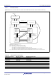
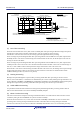
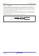
Table Of Contents
- 37. Serial Sound Interface (SSI)
- 38. Serial Peripheral Interface (RSPIa)
- 38.1 Overview
- 38.2 Register Descriptions
- 38.2.1 RSPI Control Register (SPCR)
- 38.2.2 RSPI Slave Select Polarity Register (SSLP)
- 38.2.3 RSPI Pin Control Register (SPPCR)
- 38.2.4 RSPI Status Register (SPSR)
- 38.2.5 RSPI Data Register (SPDR)
- 38.2.6 RSPI Sequence Control Register (SPSCR)
- 38.2.7 RSPI Sequence Status Register (SPSSR)
- 38.2.8 RSPI Bit Rate Register (SPBR)
- 38.2.9 RSPI Data Control Register (SPDCR)
- 38.2.10 RSPI Clock Delay Register (SPCKD)
- 38.2.11 RSPI Slave Select Negation Delay Register (SSLND)
- 38.2.12 RSPI Next-Access Delay Register (SPND)
- 38.2.13 RSPI Control Register 2 (SPCR2)
- 38.2.14 RSPI Command Register m (SPCMDm) (m = 0 to 7)
- 38.3 Operation
- 38.3.1 Overview of RSPI Operations
- 38.3.2 Controlling RSPI Pins
- 38.3.3 RSPI System Configuration Examples
- 38.3.3.1 Single Master/Single Slave (with This MCU Acting as Master)
- 38.3.3.2 Single Master/Single Slave (with This MCU Acting as Slave)
- 38.3.3.3 Single Master/Multi-Slave (with This MCU Acting as Master)
- 38.3.3.4 Single Master/Multi-Slave (with This MCU Acting as Slave)
- 38.3.3.5 Multi-Master/Multi-Slave (with This MCU Acting as Master)
- 38.3.3.6 Master (Clock Synchronous Operation)/Slave (Clock Synchronous Operation) (with This MCU Acting as Master)
- 38.3.3.7 Master (Clock Synchronous Operation)/Slave (Clock Synchronous Operation) (with This MCU Acting as Slave)
- 38.3.4 Data Format
- 38.3.5 Transfer Format
- 38.3.6 Communications Operating Mode
- 38.3.7 Transmit Buffer Empty/Receive Buffer Full Interrupts
- 38.3.8 Error Detection
- 38.3.9 Initializing RSPI
- 38.3.10 SPI Operation
- 38.3.11 Clock Synchronous Operation
- 38.3.12 Loopback Mode
- 38.3.13 Self-Diagnosis of Parity Bit Function
- 38.3.14 Interrupt Sources
- 38.4 Link Operation by Event Linking
- 38.5 Usage Notes
- 39. CRC Calculator (CRC)
- 40. SD Host Interface (SDHIa)
- 40.1 Overview
- 40.2 Register Details
- 40.2.1 Command Register (SDCMD)
- 40.2.2 Argument Register (SDARG)
- 40.2.3 Data Stop Register (SDSTOP)
- 40.2.4 Block Count Register (SDBLKCNT)
- 40.2.5 Response Register 10 (SDRSP10), Response Register 32 (SDRSP32), Response Register 54 (SDRSP54), Response Register 76 (SDRSP76)
- 40.2.6 SD Status Register 1 (SDSTS1)
- 40.2.7 SD Status Register 2 (SDSTS2)
- 40.2.8 SD Interrupt Mask Register 1 (SDIMSK1)
- 40.2.9 SD Interrupt Mask Register 2 (SDIMSK2)
- 40.2.10 SDHI Clock Control Register (SDCLKCR)
- 40.2.11 Transfer Data Size Register (SDSIZE)
- 40.2.12 Card Access Option Register (SDOPT)
- 40.2.13 SD Error Status Register 1 (SDERSTS1)
- 40.2.14 SD Error Status Register 2 (SDERSTS2)
- 40.2.15 SD Buffer Register (SDBUFR)
- 40.2.16 SDIO Mode Control Register (SDIOMD)
- 40.2.17 SDIO Status Register (SDIOSTS)
- 40.2.18 SDIO Interrupt Mask Register (SDIOIMSK)
- 40.2.19 DMA Transfer Enable Register (SDDMAEN)
- 40.2.20 SDHI Software Reset Register (SDRST)
- 40.2.21 Swap Control Register (SDSWAP)
- 40.3 SDHI Operation
- 40.3.1 Data Block Format of the SD Card
- 40.3.2 SD Buffer and the SDBUFR Register
- 40.3.3 SD Card Detection
- 40.3.4 SD Card Write Protection
- 40.3.5 Communication Errors and Timeouts
- 40.3.6 Examples of Issuing a Command
- 40.3.6.1 Command Absent of Response Reception and Data Transfer
- 40.3.6.2 Command Absent of Data Transfer
- 40.3.6.3 Single Block Read Command (CMD17)
- 40.3.6.4 Single Block Write Command (CMD24)
- 40.3.6.5 Multi-Block Read Command (CMD18)
- 40.3.6.6 Multi-Block Write Command (CMD25)
- 40.3.6.7 IO_RW_DIRECT Command (CMD52)
- 40.3.6.8 IO_RW_EXTENDED Command (CMD53 (Multi-Block Read))
- 40.3.6.9 IO_RW_EXTENDED (CMD53 Multi-Block Write)
- 40.3.6.10 DMA Transfer
- 40.4 Interrupts
- 40.5 Notes on Using the SDHI
- 40.5.1 Illegal Read Access During a Multi-Block Read and How To Avoid It
- 40.5.2 SDBUFR Register Illegal Write Error
- 40.5.3 Automatic Control of the SDHI Clock Output
- 40.5.4 Restrictions on Setting the C52PUB Bit During a Multi-Block Write Sequence
- 40.5.5 Note on Setting the SDCLKCR Register
- 40.5.6 Writing to the SDSTOP Register During a Multi-Block Read Sequence
- 40.5.7 Controlling Module Operation
- 41. Bluetooth Low Energy (BLE)
- 42. Trusted Secure IP (TSIP-Lite)
- 43. Capacitive Touch Sensing Unit (CTSU)
- 43.1 Overview
- 43.2 Register Descriptions
- 43.2.1 CTSU Control Register 0 (CTSUCR0)
- 43.2.2 CTSU Control Register 1 (CTSUCR1)
- 43.2.3 CTSU Synchronous Noise Reduction Setting Register (CTSUSDPRS)
- 43.2.4 CTSU Sensor Stabilization Wait Control Register (CTSUSST)
- 43.2.5 CTSU Measurement Channel Register 0 (CTSUMCH0)
- 43.2.6 CTSU Measurement Channel Register 1 (CTSUMCH1)
- 43.2.7 CTSU Channel Enable Control Register 0 (CTSUCHAC0)
- 43.2.8 CTSU Channel Enable Control Register 1 (CTSUCHAC1)
- 43.2.9 CTSU Channel Enable Control Register 2 (CTSUCHAC2)
- 43.2.10 CTSU Channel Enable Control Register 3 (CTSUCHAC3)
- 43.2.11 CTSU Channel Enable Control Register 4 (CTSUCHAC4)
- 43.2.12 CTSU Channel Transmit/Receive Control Register 0 (CTSUCHTRC0)
- 43.2.13 CTSU Channel Transmit/Receive Control Register 1 (CTSUCHTRC1)
- 43.2.14 CTSU Channel Transmit/Receive Control Register 2 (CTSUCHTRC2)
- 43.2.15 CTSU Channel Transmit/Receive Control Register 3 (CTSUCHTRC3)
- 43.2.16 CTSU Channel Transmit/Receive Control Register 4 (CTSUCHTRC4)
- 43.2.17 CTSU High-Pass Noise Reduction Control Register (CTSUDCLKC)
- 43.2.18 CTSU Status Register (CTSUST)
- 43.2.19 CTSU High-Pass Noise Reduction Spectrum Diffusion Control Register (CTSUSSC)
- 43.2.20 CTSU Sensor Offset Register 0 (CTSUSO0)
- 43.2.21 CTSU Sensor Offset Register 1 (CTSUSO1)
- 43.2.22 CTSU Sensor Counter (CTSUSC)
- 43.2.23 CTSU Reference Counter (CTSURC)
- 43.2.24 CTSU Error Status Register (CTSUERRS)
- 43.3 Operation
- 43.4 Usage Notes
- 44. 12-Bit A/D Converter (S12ADE)
- 44.1 Overview
- 44.2 Register Descriptions
- 44.2.1 A/D Data Registers y (ADDRy) (y = 0 to 7, 16 to 20, 27), A/D Data Duplication Register (ADDBLDR), A/D Temperature Sensor Data Register (ADTSDR), A/D Internal Reference Voltage Data Register (ADOCDR)
- 44.2.2 A/D Self-Diagnosis Data Register (ADRD)
- 44.2.3 A/D Control Register (ADCSR)
- 44.2.4 A/D Channel Select Register A0 (ADANSA0)
- 44.2.5 A/D Channel Select Register A1 (ADANSA1)
- 44.2.6 A/D Channel Select Register B0 (ADANSB0)
- 44.2.7 A/D Channel Select Register B1 (ADANSB1)
- 44.2.8 A/D-Converted Value Addition/Average Function Select Register 0 (ADADS0)
- 44.2.9 A/D-Converted Value Addition/Average Function Select Register 1 (ADADS1)
- 44.2.10 A/D-Converted Value Addition/Average Count Select Register (ADADC)
- 44.2.11 A/D Control Extended Register (ADCER)
- 44.2.12 A/D Conversion Start Trigger Select Register (ADSTRGR)
- 44.2.13 A/D Conversion Extended Input Control Register (ADEXICR)
- 44.2.14 A/D Sampling State Register n (ADSSTRn) (n = 0 to 7, L, T, O)
- 44.2.15 A/D Disconnection Detection Control Register (ADDISCR)
- 44.2.16 A/D Event Link Control Register (ADELCCR)
- 44.2.17 A/D Group Scan Priority Control Register (ADGSPCR)
- 44.2.18 A/D Compare Function Control Register (ADCMPCR)
- 44.2.19 A/D Compare Function Window A Channel Select Register 0 (ADCMPANSR0)
- 44.2.20 A/D Compare Function Window A Channel Select Register 1 (ADCMPANSR1)
- 44.2.21 A/D Compare Function Window A Extended Input Select Register (ADCMPANSER)
- 44.2.22 A/D Compare Function Window A Comparison Condition Setting Register 0 (ADCMPLR0)
- 44.2.23 A/D Compare Function Window A Comparison Condition Setting Register 1 (ADCMPLR1)
- 44.2.24 A/D Compare Function Window A Extended Input Comparison Condition Setting Register (ADCMPLER)
- 44.2.25 A/D Compare Function Window A Lower-Side Level Setting Register (ADCMPDR0)
- 44.2.26 A/D Compare Function Window A Upper-Side Level Setting Register (ADCMPDR1)
- 44.2.27 A/D Compare Function Window A Channel Status Register 0 (ADCMPSR0)
- 44.2.28 A/D Compare Function Window A Channel Status Register 1 (ADCMPSR1)
- 44.2.29 A/D Compare Function Window A Extended Input Channel Status Register (ADCMPSER)
- 44.2.30 A/D High-Potential/Low-Potential Reference Voltage Control Register (ADHVREFCNT)
- 44.2.31 A/D Compare Function Window A/B Status Monitor Register (ADWINMON)
- 44.2.32 A/D Compare Function Window B Channel Select Register (ADCMPBNSR)
- 44.2.33 A/D Compare Function Window B Lower-Side Level Setting Register (ADWINLLB)
- 44.2.34 A/D Compare Function Window B Upper-Side Level Setting Register (ADWINULB)
- 44.2.35 A/D Compare Function Window B Channel Status Register (ADCMPBSR)
- 44.2.36 A/D Data Storage Buffer Register n (ADBUFn) (n = 0 to 15)

R01UH0823EJ0110 Rev.1.10 Page 1277 of 1852
Nov 30, 2020
RX23W Group 36. CAN Module (RSCAN)
Figure 36.5 Acceptance Filter Function
(2) DLC Filter Processing
When the GCFGL.DCE bit is set to 1 (DLC check is enabled), DLC filter processing is added to messages that passed
through the acceptance filter processing. When the DLC value in a message is equal to or larger
than the DLC value set in the receive rule, the message passes through the DLC filter processing.
When a message has passed through the DLC filter processing with the GCFGL.DRE bit set to 0 (DLC replacement is
disabled), the DLC value in the received message is stored in the buffer. In this case, all the data bytes in the received
message are stored in the buffer.
When a message has passed through the DLC filter processing with the GCFGL.DRE bit set to 1 (DLC replacement is
enabled), the DLC value in the receive rule is stored in the buffer instead of the DLC value in the received message. In
this case, a value of 00h is written to data bytes that are larger than the DLC value in the receive rule.
When the DLC value in the received message is smaller than that in the receive rule, the message does not pass through
the DLC filter processing. In this case, the message is not stored in the receive buffer or the FIFO buffer and the
GERFLL.DEF flag becomes 1 (a DLC error is present).
(3) Routing Processing
Messages that passed through the acceptance filter processing and the DLC filter processing are stored in receive
buffers, receive FIFO buffers, or transmit/receive FIFO buffers (set to receive mode). Message storage destination is set
by the GAFLPLj.GAFLRMV, GAFLRMDP[6:0], GAFLFDP4, GAFLFDP1, and GAFLFDP0 bits. Messages that passed
through the acceptance filter processing and the DLC filter processing can be stored in up to two buffers.
(4) Label Addition Processing
It is possible to add 12-bit label information to messages that passed through the filter processing and store them in
buffers. This label information is set in the GAFLPHj.GAFLPTR[11:0] bits.
(5) Mirror Function Processing
The mirror function allows reception of messages transmitted from the own CAN node. The mirror function is made
available by setting the GCFGL.MME bit to 1 (mirror function is enabled).
When the mirror function is in use, receive rules for which the GAFLIDHj.GAFLLB bit is set to 0 are used for data
processing when receiving messages transmitted from other CAN nodes. When receiving messages transmitted
from the own CAN node, receive rules for which the GAFLIDHj.GAFLLB bit is set to 1 are used for data processing.
ID value in
received message
GAFLIDHj, GAFLIDLj
(receive rule entry register jAH/AL)
GAFLMHj, GAFLMLj
(receive rule entry register jBH/BL)
GAFL
IDE
GAFL
RTR
GAFLID
GAFL
IDEM
GAFL
RTRM
GAFLIDM
Acceptance
determination signal
Mask bit value
0: Bits are not compared.
1: Bits are compared.
Acceptance determination signal
0: Does not pass the acceptance filter processing.
(Not stored in the buffer)
1: Passes the acceptance filter processing.
GAFLIDE, GAFLRTR, GAFLID: Bits in the GAFLIDHj and GAFLIDLj registers
GAFLIDEM, GAFLRTRM, GAFLIDM: Mask bits in the GAFLMHj and GAFLMLj registers