
Users Manual
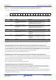
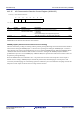
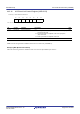
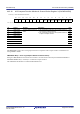
Table Of Contents
- 37. Serial Sound Interface (SSI)
- 38. Serial Peripheral Interface (RSPIa)
- 38.1 Overview
- 38.2 Register Descriptions
- 38.2.1 RSPI Control Register (SPCR)
- 38.2.2 RSPI Slave Select Polarity Register (SSLP)
- 38.2.3 RSPI Pin Control Register (SPPCR)
- 38.2.4 RSPI Status Register (SPSR)
- 38.2.5 RSPI Data Register (SPDR)
- 38.2.6 RSPI Sequence Control Register (SPSCR)
- 38.2.7 RSPI Sequence Status Register (SPSSR)
- 38.2.8 RSPI Bit Rate Register (SPBR)
- 38.2.9 RSPI Data Control Register (SPDCR)
- 38.2.10 RSPI Clock Delay Register (SPCKD)
- 38.2.11 RSPI Slave Select Negation Delay Register (SSLND)
- 38.2.12 RSPI Next-Access Delay Register (SPND)
- 38.2.13 RSPI Control Register 2 (SPCR2)
- 38.2.14 RSPI Command Register m (SPCMDm) (m = 0 to 7)
- 38.3 Operation
- 38.3.1 Overview of RSPI Operations
- 38.3.2 Controlling RSPI Pins
- 38.3.3 RSPI System Configuration Examples
- 38.3.3.1 Single Master/Single Slave (with This MCU Acting as Master)
- 38.3.3.2 Single Master/Single Slave (with This MCU Acting as Slave)
- 38.3.3.3 Single Master/Multi-Slave (with This MCU Acting as Master)
- 38.3.3.4 Single Master/Multi-Slave (with This MCU Acting as Slave)
- 38.3.3.5 Multi-Master/Multi-Slave (with This MCU Acting as Master)
- 38.3.3.6 Master (Clock Synchronous Operation)/Slave (Clock Synchronous Operation) (with This MCU Acting as Master)
- 38.3.3.7 Master (Clock Synchronous Operation)/Slave (Clock Synchronous Operation) (with This MCU Acting as Slave)
- 38.3.4 Data Format
- 38.3.5 Transfer Format
- 38.3.6 Communications Operating Mode
- 38.3.7 Transmit Buffer Empty/Receive Buffer Full Interrupts
- 38.3.8 Error Detection
- 38.3.9 Initializing RSPI
- 38.3.10 SPI Operation
- 38.3.11 Clock Synchronous Operation
- 38.3.12 Loopback Mode
- 38.3.13 Self-Diagnosis of Parity Bit Function
- 38.3.14 Interrupt Sources
- 38.4 Link Operation by Event Linking
- 38.5 Usage Notes
- 39. CRC Calculator (CRC)
- 40. SD Host Interface (SDHIa)
- 40.1 Overview
- 40.2 Register Details
- 40.2.1 Command Register (SDCMD)
- 40.2.2 Argument Register (SDARG)
- 40.2.3 Data Stop Register (SDSTOP)
- 40.2.4 Block Count Register (SDBLKCNT)
- 40.2.5 Response Register 10 (SDRSP10), Response Register 32 (SDRSP32), Response Register 54 (SDRSP54), Response Register 76 (SDRSP76)
- 40.2.6 SD Status Register 1 (SDSTS1)
- 40.2.7 SD Status Register 2 (SDSTS2)
- 40.2.8 SD Interrupt Mask Register 1 (SDIMSK1)
- 40.2.9 SD Interrupt Mask Register 2 (SDIMSK2)
- 40.2.10 SDHI Clock Control Register (SDCLKCR)
- 40.2.11 Transfer Data Size Register (SDSIZE)
- 40.2.12 Card Access Option Register (SDOPT)
- 40.2.13 SD Error Status Register 1 (SDERSTS1)
- 40.2.14 SD Error Status Register 2 (SDERSTS2)
- 40.2.15 SD Buffer Register (SDBUFR)
- 40.2.16 SDIO Mode Control Register (SDIOMD)
- 40.2.17 SDIO Status Register (SDIOSTS)
- 40.2.18 SDIO Interrupt Mask Register (SDIOIMSK)
- 40.2.19 DMA Transfer Enable Register (SDDMAEN)
- 40.2.20 SDHI Software Reset Register (SDRST)
- 40.2.21 Swap Control Register (SDSWAP)
- 40.3 SDHI Operation
- 40.3.1 Data Block Format of the SD Card
- 40.3.2 SD Buffer and the SDBUFR Register
- 40.3.3 SD Card Detection
- 40.3.4 SD Card Write Protection
- 40.3.5 Communication Errors and Timeouts
- 40.3.6 Examples of Issuing a Command
- 40.3.6.1 Command Absent of Response Reception and Data Transfer
- 40.3.6.2 Command Absent of Data Transfer
- 40.3.6.3 Single Block Read Command (CMD17)
- 40.3.6.4 Single Block Write Command (CMD24)
- 40.3.6.5 Multi-Block Read Command (CMD18)
- 40.3.6.6 Multi-Block Write Command (CMD25)
- 40.3.6.7 IO_RW_DIRECT Command (CMD52)
- 40.3.6.8 IO_RW_EXTENDED Command (CMD53 (Multi-Block Read))
- 40.3.6.9 IO_RW_EXTENDED (CMD53 Multi-Block Write)
- 40.3.6.10 DMA Transfer
- 40.4 Interrupts
- 40.5 Notes on Using the SDHI
- 40.5.1 Illegal Read Access During a Multi-Block Read and How To Avoid It
- 40.5.2 SDBUFR Register Illegal Write Error
- 40.5.3 Automatic Control of the SDHI Clock Output
- 40.5.4 Restrictions on Setting the C52PUB Bit During a Multi-Block Write Sequence
- 40.5.5 Note on Setting the SDCLKCR Register
- 40.5.6 Writing to the SDSTOP Register During a Multi-Block Read Sequence
- 40.5.7 Controlling Module Operation
- 41. Bluetooth Low Energy (BLE)
- 42. Trusted Secure IP (TSIP-Lite)
- 43. Capacitive Touch Sensing Unit (CTSU)
- 43.1 Overview
- 43.2 Register Descriptions
- 43.2.1 CTSU Control Register 0 (CTSUCR0)
- 43.2.2 CTSU Control Register 1 (CTSUCR1)
- 43.2.3 CTSU Synchronous Noise Reduction Setting Register (CTSUSDPRS)
- 43.2.4 CTSU Sensor Stabilization Wait Control Register (CTSUSST)
- 43.2.5 CTSU Measurement Channel Register 0 (CTSUMCH0)
- 43.2.6 CTSU Measurement Channel Register 1 (CTSUMCH1)
- 43.2.7 CTSU Channel Enable Control Register 0 (CTSUCHAC0)
- 43.2.8 CTSU Channel Enable Control Register 1 (CTSUCHAC1)
- 43.2.9 CTSU Channel Enable Control Register 2 (CTSUCHAC2)
- 43.2.10 CTSU Channel Enable Control Register 3 (CTSUCHAC3)
- 43.2.11 CTSU Channel Enable Control Register 4 (CTSUCHAC4)
- 43.2.12 CTSU Channel Transmit/Receive Control Register 0 (CTSUCHTRC0)
- 43.2.13 CTSU Channel Transmit/Receive Control Register 1 (CTSUCHTRC1)
- 43.2.14 CTSU Channel Transmit/Receive Control Register 2 (CTSUCHTRC2)
- 43.2.15 CTSU Channel Transmit/Receive Control Register 3 (CTSUCHTRC3)
- 43.2.16 CTSU Channel Transmit/Receive Control Register 4 (CTSUCHTRC4)
- 43.2.17 CTSU High-Pass Noise Reduction Control Register (CTSUDCLKC)
- 43.2.18 CTSU Status Register (CTSUST)
- 43.2.19 CTSU High-Pass Noise Reduction Spectrum Diffusion Control Register (CTSUSSC)
- 43.2.20 CTSU Sensor Offset Register 0 (CTSUSO0)
- 43.2.21 CTSU Sensor Offset Register 1 (CTSUSO1)
- 43.2.22 CTSU Sensor Counter (CTSUSC)
- 43.2.23 CTSU Reference Counter (CTSURC)
- 43.2.24 CTSU Error Status Register (CTSUERRS)
- 43.3 Operation
- 43.4 Usage Notes
- 44. 12-Bit A/D Converter (S12ADE)
- 44.1 Overview
- 44.2 Register Descriptions
- 44.2.1 A/D Data Registers y (ADDRy) (y = 0 to 7, 16 to 20, 27), A/D Data Duplication Register (ADDBLDR), A/D Temperature Sensor Data Register (ADTSDR), A/D Internal Reference Voltage Data Register (ADOCDR)
- 44.2.2 A/D Self-Diagnosis Data Register (ADRD)
- 44.2.3 A/D Control Register (ADCSR)
- 44.2.4 A/D Channel Select Register A0 (ADANSA0)
- 44.2.5 A/D Channel Select Register A1 (ADANSA1)
- 44.2.6 A/D Channel Select Register B0 (ADANSB0)
- 44.2.7 A/D Channel Select Register B1 (ADANSB1)
- 44.2.8 A/D-Converted Value Addition/Average Function Select Register 0 (ADADS0)
- 44.2.9 A/D-Converted Value Addition/Average Function Select Register 1 (ADADS1)
- 44.2.10 A/D-Converted Value Addition/Average Count Select Register (ADADC)
- 44.2.11 A/D Control Extended Register (ADCER)
- 44.2.12 A/D Conversion Start Trigger Select Register (ADSTRGR)
- 44.2.13 A/D Conversion Extended Input Control Register (ADEXICR)
- 44.2.14 A/D Sampling State Register n (ADSSTRn) (n = 0 to 7, L, T, O)
- 44.2.15 A/D Disconnection Detection Control Register (ADDISCR)
- 44.2.16 A/D Event Link Control Register (ADELCCR)
- 44.2.17 A/D Group Scan Priority Control Register (ADGSPCR)
- 44.2.18 A/D Compare Function Control Register (ADCMPCR)
- 44.2.19 A/D Compare Function Window A Channel Select Register 0 (ADCMPANSR0)
- 44.2.20 A/D Compare Function Window A Channel Select Register 1 (ADCMPANSR1)
- 44.2.21 A/D Compare Function Window A Extended Input Select Register (ADCMPANSER)
- 44.2.22 A/D Compare Function Window A Comparison Condition Setting Register 0 (ADCMPLR0)
- 44.2.23 A/D Compare Function Window A Comparison Condition Setting Register 1 (ADCMPLR1)
- 44.2.24 A/D Compare Function Window A Extended Input Comparison Condition Setting Register (ADCMPLER)
- 44.2.25 A/D Compare Function Window A Lower-Side Level Setting Register (ADCMPDR0)
- 44.2.26 A/D Compare Function Window A Upper-Side Level Setting Register (ADCMPDR1)
- 44.2.27 A/D Compare Function Window A Channel Status Register 0 (ADCMPSR0)
- 44.2.28 A/D Compare Function Window A Channel Status Register 1 (ADCMPSR1)
- 44.2.29 A/D Compare Function Window A Extended Input Channel Status Register (ADCMPSER)
- 44.2.30 A/D High-Potential/Low-Potential Reference Voltage Control Register (ADHVREFCNT)
- 44.2.31 A/D Compare Function Window A/B Status Monitor Register (ADWINMON)
- 44.2.32 A/D Compare Function Window B Channel Select Register (ADCMPBNSR)
- 44.2.33 A/D Compare Function Window B Lower-Side Level Setting Register (ADWINLLB)
- 44.2.34 A/D Compare Function Window B Upper-Side Level Setting Register (ADWINULB)
- 44.2.35 A/D Compare Function Window B Channel Status Register (ADCMPBSR)
- 44.2.36 A/D Data Storage Buffer Register n (ADBUFn) (n = 0 to 15)

R01UH0823EJ0110 Rev.1.10 Page 1576 of 1852
Nov 30, 2020
RX23W Group 44. 12-Bit A/D Converter (S12ADE)
44.2.17 A/D Group Scan Priority Control Register (ADGSPCR)
Note 1. When the PGS bit is to be set to 1, the ADCSR.ADCS[1:0] bits must be set to 01b (group scan mode). If the bits are set to any
other values, proper operation is not guaranteed.
Note 2. When the GBRSCN bit is to be set to 1, the frequency ratio of peripheral module clock PCLK to A/D conversion clock ADCLK
should be set to 1:1.
Note 3. When the GBRP bit has been set to 1, single scan is performed continuously for group B regardless of the setting of the
GBRSCN bit.
ADGSPCR is used to make settings for priority control of A/D conversion for group A in group scan mode.
PGS Bit (Group-A Priority Control Setting)
This bit sets the priority of operation on group A. Set this bit to 1 when giving priority to operation on group A.
When the PGS bit is to be set to 1, the ADCSR.ADCS[1:0] bits must be set to 01b (group scan mode).
When setting the PGS bit to 0, clearing should be performed by software according to
section 44.8.2, Notes on
Stopping A/D Conversion
. When setting the PGS bit to 1, follow the procedure described in section 44.3.4.3,
Operation under Group-A Priority Control
.
GBRSCN Bit (Group B Restart Setting)
This bit controls the restarting of scan operation on group B when operation on group A is given priority.
If a scan operation on group B has been stopped by a group A trigger input with the GBRSCN bit set to 1, the scan
operation is restarted on completion of the A/D conversion on group A. Also, if a group B trigger is input during A/D
conversion on group A, the scan operation on group B is restarted on completion of the A/D conversion on group A.
If the GBRSCN bit has been set to 0, triggers that are input during A/D conversion are ignored. Also, the ADCSR.ADST
bit must be 0 when the GBRSCN bit is to be set.
The setting of the GBRSCN bit is enabled when the PGS bit is set to 1.
GBRP Bit (Group B Single Scan Continuous Start)
This bit is set when a single scan operation is to be performed continuously on group B.
Setting the GBRP bit to 1 starts a single scan on group B. On completion of the scan, another single scan on group B is
automatically started. If an A/D conversion on group B has been stopped due to an operation on group A that takes
priority, single scan on group B is automatically restarted on completion of the A/D conversion on group A.
Disable group B trigger input before setting the GBRP bit to 1. Setting the GBRP bit to 1 invalidates the setting of the
Address(es): S12AD.ADGSPCR 0008 9080h
b15 b14 b13 b12 b11 b10 b9 b8 b7 b6 b5 b4 b3 b2 b1 b0
GBRP—————————————
GBRSC
N
PGS
Value after reset:
0000000000000000
Bit Symbol Bit Name Description R/W
b0 PGS Group-A Priority
Control Setting
*
1
0: Operation is without group-A priority control
1: Operation is with group-A priority control
R/W
b1 GBRSCN Group B Restart
Setting
*
2
(Enabled only when PGS = 1. Reserved when PGS = 0.)
0: Scanning for group B is not restarted after having been discontinued due
to group-A priority control.
1: Scanning for group B is restarted after having been discontinued due to
group-A priority control.
R/W
b14 to b2 — Reserved These bits are read as 0. The write value should be 0. R/W
b15 GBRP Group B Single Scan
Continuous Start
*
3
(Enabled only when PGS = 1. Reserved when PGS = 0.)
0: Single scan for group B is not continuously activated.
1: Single scan for group B is continuously activated.
R/W