
Users Manual
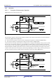
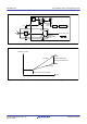
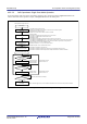
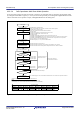
Table Of Contents
- 37. Serial Sound Interface (SSI)
- 38. Serial Peripheral Interface (RSPIa)
- 38.1 Overview
- 38.2 Register Descriptions
- 38.2.1 RSPI Control Register (SPCR)
- 38.2.2 RSPI Slave Select Polarity Register (SSLP)
- 38.2.3 RSPI Pin Control Register (SPPCR)
- 38.2.4 RSPI Status Register (SPSR)
- 38.2.5 RSPI Data Register (SPDR)
- 38.2.6 RSPI Sequence Control Register (SPSCR)
- 38.2.7 RSPI Sequence Status Register (SPSSR)
- 38.2.8 RSPI Bit Rate Register (SPBR)
- 38.2.9 RSPI Data Control Register (SPDCR)
- 38.2.10 RSPI Clock Delay Register (SPCKD)
- 38.2.11 RSPI Slave Select Negation Delay Register (SSLND)
- 38.2.12 RSPI Next-Access Delay Register (SPND)
- 38.2.13 RSPI Control Register 2 (SPCR2)
- 38.2.14 RSPI Command Register m (SPCMDm) (m = 0 to 7)
- 38.3 Operation
- 38.3.1 Overview of RSPI Operations
- 38.3.2 Controlling RSPI Pins
- 38.3.3 RSPI System Configuration Examples
- 38.3.3.1 Single Master/Single Slave (with This MCU Acting as Master)
- 38.3.3.2 Single Master/Single Slave (with This MCU Acting as Slave)
- 38.3.3.3 Single Master/Multi-Slave (with This MCU Acting as Master)
- 38.3.3.4 Single Master/Multi-Slave (with This MCU Acting as Slave)
- 38.3.3.5 Multi-Master/Multi-Slave (with This MCU Acting as Master)
- 38.3.3.6 Master (Clock Synchronous Operation)/Slave (Clock Synchronous Operation) (with This MCU Acting as Master)
- 38.3.3.7 Master (Clock Synchronous Operation)/Slave (Clock Synchronous Operation) (with This MCU Acting as Slave)
- 38.3.4 Data Format
- 38.3.5 Transfer Format
- 38.3.6 Communications Operating Mode
- 38.3.7 Transmit Buffer Empty/Receive Buffer Full Interrupts
- 38.3.8 Error Detection
- 38.3.9 Initializing RSPI
- 38.3.10 SPI Operation
- 38.3.11 Clock Synchronous Operation
- 38.3.12 Loopback Mode
- 38.3.13 Self-Diagnosis of Parity Bit Function
- 38.3.14 Interrupt Sources
- 38.4 Link Operation by Event Linking
- 38.5 Usage Notes
- 39. CRC Calculator (CRC)
- 40. SD Host Interface (SDHIa)
- 40.1 Overview
- 40.2 Register Details
- 40.2.1 Command Register (SDCMD)
- 40.2.2 Argument Register (SDARG)
- 40.2.3 Data Stop Register (SDSTOP)
- 40.2.4 Block Count Register (SDBLKCNT)
- 40.2.5 Response Register 10 (SDRSP10), Response Register 32 (SDRSP32), Response Register 54 (SDRSP54), Response Register 76 (SDRSP76)
- 40.2.6 SD Status Register 1 (SDSTS1)
- 40.2.7 SD Status Register 2 (SDSTS2)
- 40.2.8 SD Interrupt Mask Register 1 (SDIMSK1)
- 40.2.9 SD Interrupt Mask Register 2 (SDIMSK2)
- 40.2.10 SDHI Clock Control Register (SDCLKCR)
- 40.2.11 Transfer Data Size Register (SDSIZE)
- 40.2.12 Card Access Option Register (SDOPT)
- 40.2.13 SD Error Status Register 1 (SDERSTS1)
- 40.2.14 SD Error Status Register 2 (SDERSTS2)
- 40.2.15 SD Buffer Register (SDBUFR)
- 40.2.16 SDIO Mode Control Register (SDIOMD)
- 40.2.17 SDIO Status Register (SDIOSTS)
- 40.2.18 SDIO Interrupt Mask Register (SDIOIMSK)
- 40.2.19 DMA Transfer Enable Register (SDDMAEN)
- 40.2.20 SDHI Software Reset Register (SDRST)
- 40.2.21 Swap Control Register (SDSWAP)
- 40.3 SDHI Operation
- 40.3.1 Data Block Format of the SD Card
- 40.3.2 SD Buffer and the SDBUFR Register
- 40.3.3 SD Card Detection
- 40.3.4 SD Card Write Protection
- 40.3.5 Communication Errors and Timeouts
- 40.3.6 Examples of Issuing a Command
- 40.3.6.1 Command Absent of Response Reception and Data Transfer
- 40.3.6.2 Command Absent of Data Transfer
- 40.3.6.3 Single Block Read Command (CMD17)
- 40.3.6.4 Single Block Write Command (CMD24)
- 40.3.6.5 Multi-Block Read Command (CMD18)
- 40.3.6.6 Multi-Block Write Command (CMD25)
- 40.3.6.7 IO_RW_DIRECT Command (CMD52)
- 40.3.6.8 IO_RW_EXTENDED Command (CMD53 (Multi-Block Read))
- 40.3.6.9 IO_RW_EXTENDED (CMD53 Multi-Block Write)
- 40.3.6.10 DMA Transfer
- 40.4 Interrupts
- 40.5 Notes on Using the SDHI
- 40.5.1 Illegal Read Access During a Multi-Block Read and How To Avoid It
- 40.5.2 SDBUFR Register Illegal Write Error
- 40.5.3 Automatic Control of the SDHI Clock Output
- 40.5.4 Restrictions on Setting the C52PUB Bit During a Multi-Block Write Sequence
- 40.5.5 Note on Setting the SDCLKCR Register
- 40.5.6 Writing to the SDSTOP Register During a Multi-Block Read Sequence
- 40.5.7 Controlling Module Operation
- 41. Bluetooth Low Energy (BLE)
- 42. Trusted Secure IP (TSIP-Lite)
- 43. Capacitive Touch Sensing Unit (CTSU)
- 43.1 Overview
- 43.2 Register Descriptions
- 43.2.1 CTSU Control Register 0 (CTSUCR0)
- 43.2.2 CTSU Control Register 1 (CTSUCR1)
- 43.2.3 CTSU Synchronous Noise Reduction Setting Register (CTSUSDPRS)
- 43.2.4 CTSU Sensor Stabilization Wait Control Register (CTSUSST)
- 43.2.5 CTSU Measurement Channel Register 0 (CTSUMCH0)
- 43.2.6 CTSU Measurement Channel Register 1 (CTSUMCH1)
- 43.2.7 CTSU Channel Enable Control Register 0 (CTSUCHAC0)
- 43.2.8 CTSU Channel Enable Control Register 1 (CTSUCHAC1)
- 43.2.9 CTSU Channel Enable Control Register 2 (CTSUCHAC2)
- 43.2.10 CTSU Channel Enable Control Register 3 (CTSUCHAC3)
- 43.2.11 CTSU Channel Enable Control Register 4 (CTSUCHAC4)
- 43.2.12 CTSU Channel Transmit/Receive Control Register 0 (CTSUCHTRC0)
- 43.2.13 CTSU Channel Transmit/Receive Control Register 1 (CTSUCHTRC1)
- 43.2.14 CTSU Channel Transmit/Receive Control Register 2 (CTSUCHTRC2)
- 43.2.15 CTSU Channel Transmit/Receive Control Register 3 (CTSUCHTRC3)
- 43.2.16 CTSU Channel Transmit/Receive Control Register 4 (CTSUCHTRC4)
- 43.2.17 CTSU High-Pass Noise Reduction Control Register (CTSUDCLKC)
- 43.2.18 CTSU Status Register (CTSUST)
- 43.2.19 CTSU High-Pass Noise Reduction Spectrum Diffusion Control Register (CTSUSSC)
- 43.2.20 CTSU Sensor Offset Register 0 (CTSUSO0)
- 43.2.21 CTSU Sensor Offset Register 1 (CTSUSO1)
- 43.2.22 CTSU Sensor Counter (CTSUSC)
- 43.2.23 CTSU Reference Counter (CTSURC)
- 43.2.24 CTSU Error Status Register (CTSUERRS)
- 43.3 Operation
- 43.4 Usage Notes
- 44. 12-Bit A/D Converter (S12ADE)
- 44.1 Overview
- 44.2 Register Descriptions
- 44.2.1 A/D Data Registers y (ADDRy) (y = 0 to 7, 16 to 20, 27), A/D Data Duplication Register (ADDBLDR), A/D Temperature Sensor Data Register (ADTSDR), A/D Internal Reference Voltage Data Register (ADOCDR)
- 44.2.2 A/D Self-Diagnosis Data Register (ADRD)
- 44.2.3 A/D Control Register (ADCSR)
- 44.2.4 A/D Channel Select Register A0 (ADANSA0)
- 44.2.5 A/D Channel Select Register A1 (ADANSA1)
- 44.2.6 A/D Channel Select Register B0 (ADANSB0)
- 44.2.7 A/D Channel Select Register B1 (ADANSB1)
- 44.2.8 A/D-Converted Value Addition/Average Function Select Register 0 (ADADS0)
- 44.2.9 A/D-Converted Value Addition/Average Function Select Register 1 (ADADS1)
- 44.2.10 A/D-Converted Value Addition/Average Count Select Register (ADADC)
- 44.2.11 A/D Control Extended Register (ADCER)
- 44.2.12 A/D Conversion Start Trigger Select Register (ADSTRGR)
- 44.2.13 A/D Conversion Extended Input Control Register (ADEXICR)
- 44.2.14 A/D Sampling State Register n (ADSSTRn) (n = 0 to 7, L, T, O)
- 44.2.15 A/D Disconnection Detection Control Register (ADDISCR)
- 44.2.16 A/D Event Link Control Register (ADELCCR)
- 44.2.17 A/D Group Scan Priority Control Register (ADGSPCR)
- 44.2.18 A/D Compare Function Control Register (ADCMPCR)
- 44.2.19 A/D Compare Function Window A Channel Select Register 0 (ADCMPANSR0)
- 44.2.20 A/D Compare Function Window A Channel Select Register 1 (ADCMPANSR1)
- 44.2.21 A/D Compare Function Window A Extended Input Select Register (ADCMPANSER)
- 44.2.22 A/D Compare Function Window A Comparison Condition Setting Register 0 (ADCMPLR0)
- 44.2.23 A/D Compare Function Window A Comparison Condition Setting Register 1 (ADCMPLR1)
- 44.2.24 A/D Compare Function Window A Extended Input Comparison Condition Setting Register (ADCMPLER)
- 44.2.25 A/D Compare Function Window A Lower-Side Level Setting Register (ADCMPDR0)
- 44.2.26 A/D Compare Function Window A Upper-Side Level Setting Register (ADCMPDR1)
- 44.2.27 A/D Compare Function Window A Channel Status Register 0 (ADCMPSR0)
- 44.2.28 A/D Compare Function Window A Channel Status Register 1 (ADCMPSR1)
- 44.2.29 A/D Compare Function Window A Extended Input Channel Status Register (ADCMPSER)
- 44.2.30 A/D High-Potential/Low-Potential Reference Voltage Control Register (ADHVREFCNT)
- 44.2.31 A/D Compare Function Window A/B Status Monitor Register (ADWINMON)
- 44.2.32 A/D Compare Function Window B Channel Select Register (ADCMPBNSR)
- 44.2.33 A/D Compare Function Window B Lower-Side Level Setting Register (ADWINLLB)
- 44.2.34 A/D Compare Function Window B Upper-Side Level Setting Register (ADWINULB)
- 44.2.35 A/D Compare Function Window B Channel Status Register (ADCMPBSR)
- 44.2.36 A/D Data Storage Buffer Register n (ADBUFn) (n = 0 to 15)

R01UH0823EJ0110 Rev.1.10 Page 1535 of 1852
Nov 30, 2020
RX23W Group 43. Capacitive Touch Sensing Unit (CTSU)
43.3.2.2 Status Counter
The measurement status counter of the CTSU status register (CTSUST) indicates the current measurement status. The
measurement status is common to all four modes.
Figure 43.11 shows status operation transitions.
Figure 43.11 Status Operation Transitions
The status of the status counter transitions to Status 0 when all of the specified measurement channels are measured.
The CTSUCR0.CTSUSTRT bit is cleared to 0 by hardware when a software trigger is used. When an external trigger is
used, the value 1 is retained, and the CTSU waits for the next trigger.
When operation is forcibly stopped (by writing 0 to the CTSUCR0.CTSUSTRT bit and 1 to the CTSUCR0.CTSUINIT
bit at the same time) during measurement or the wait state for the trigger, the status transitions to Status 0 and
measurement is stopped forcibly.
If there is no channel to be measured by setting the CTSUMCH0, CTSUCHACn, and CTSUCHTRCn registers (n = 0 to
4), a CTSUFN interrupt is generated immediately after a transition to Status 1, and then the status transitions to Status 0.
The following are the cases when there is no channel to be measured.
• A measurement target channel is not specified by the CTSUCHACn registers.
• In self-capacitance single scan mode, the channel specified in the CTSUMCH0 register is not a measurement target
in the CTSUCHACn registers.
• In full scan mode, there is no transmit channel or receive channel to be measured by combining the CTSUCHACn
and CTSUCHTRCn registers.
Status 0
Stopped/wait for external trigger
Status1
Measurement channel update/
determination of measurement finish
Status 2
Wait for sensor drive pulse setting
Status 4
Measurement start/
measurement period
Conditions for transition to Status 1
• CTSUCR0.CTSUCAP bit = 0: CTSUCR0.CTSUSTRT bit = 1
• CTSUCR0.CTSUCAP bit = 1: CTSUCR0.CTSUSTRT bit = 1 and
the rising edge of the external trigger is detected
Status 5
Measurement completed
Status 3
Sensor drive pulse output start/
sensor stabilization wait period*
2
Condition for transition to Status 0
• There is no channel to be measured next
(A CTSUFN interrupt is generated and measurement is finished)
Condition for transition to Status 2
• Update of the measurement channel is completed
Condition for transition to Status 3
• CTSUST.CTSUPS flag = 1 (second measurement) in mutual capacitance
full scan mode
Condition for transition to Status 3
• Write access to the CTSUSO1 register*
1
Condition for transition to Status 4
• CTSUST.CTSUDTSR flag = 0 when the sensor stabilization has elapsed
after supply of the sensor drive pulse starts
Condition for transition to Status 5
• The measurement time has elapsed after measurement is started
For details on the measurement time, refer to the Sensor Stabilization Wait
Time and Measurement Time in the Capacitive Touch Sensor (CTSU)
section.
Condition for transition to Status 1
• After two clocks of the operating clock have elapsed
Note 1. When using the DTC/ICU to set the registers in the CTSUWR interrupt
handling, write to the CTSUSO1 register last.
Note 2. If the CTSUST.CTSUDTSR flag is 1, wait until the previous measurement
result is transferred.