
Users Manual
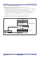
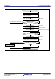
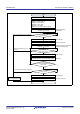
Table Of Contents
- 37. Serial Sound Interface (SSI)
- 38. Serial Peripheral Interface (RSPIa)
- 38.1 Overview
- 38.2 Register Descriptions
- 38.2.1 RSPI Control Register (SPCR)
- 38.2.2 RSPI Slave Select Polarity Register (SSLP)
- 38.2.3 RSPI Pin Control Register (SPPCR)
- 38.2.4 RSPI Status Register (SPSR)
- 38.2.5 RSPI Data Register (SPDR)
- 38.2.6 RSPI Sequence Control Register (SPSCR)
- 38.2.7 RSPI Sequence Status Register (SPSSR)
- 38.2.8 RSPI Bit Rate Register (SPBR)
- 38.2.9 RSPI Data Control Register (SPDCR)
- 38.2.10 RSPI Clock Delay Register (SPCKD)
- 38.2.11 RSPI Slave Select Negation Delay Register (SSLND)
- 38.2.12 RSPI Next-Access Delay Register (SPND)
- 38.2.13 RSPI Control Register 2 (SPCR2)
- 38.2.14 RSPI Command Register m (SPCMDm) (m = 0 to 7)
- 38.3 Operation
- 38.3.1 Overview of RSPI Operations
- 38.3.2 Controlling RSPI Pins
- 38.3.3 RSPI System Configuration Examples
- 38.3.3.1 Single Master/Single Slave (with This MCU Acting as Master)
- 38.3.3.2 Single Master/Single Slave (with This MCU Acting as Slave)
- 38.3.3.3 Single Master/Multi-Slave (with This MCU Acting as Master)
- 38.3.3.4 Single Master/Multi-Slave (with This MCU Acting as Slave)
- 38.3.3.5 Multi-Master/Multi-Slave (with This MCU Acting as Master)
- 38.3.3.6 Master (Clock Synchronous Operation)/Slave (Clock Synchronous Operation) (with This MCU Acting as Master)
- 38.3.3.7 Master (Clock Synchronous Operation)/Slave (Clock Synchronous Operation) (with This MCU Acting as Slave)
- 38.3.4 Data Format
- 38.3.5 Transfer Format
- 38.3.6 Communications Operating Mode
- 38.3.7 Transmit Buffer Empty/Receive Buffer Full Interrupts
- 38.3.8 Error Detection
- 38.3.9 Initializing RSPI
- 38.3.10 SPI Operation
- 38.3.11 Clock Synchronous Operation
- 38.3.12 Loopback Mode
- 38.3.13 Self-Diagnosis of Parity Bit Function
- 38.3.14 Interrupt Sources
- 38.4 Link Operation by Event Linking
- 38.5 Usage Notes
- 39. CRC Calculator (CRC)
- 40. SD Host Interface (SDHIa)
- 40.1 Overview
- 40.2 Register Details
- 40.2.1 Command Register (SDCMD)
- 40.2.2 Argument Register (SDARG)
- 40.2.3 Data Stop Register (SDSTOP)
- 40.2.4 Block Count Register (SDBLKCNT)
- 40.2.5 Response Register 10 (SDRSP10), Response Register 32 (SDRSP32), Response Register 54 (SDRSP54), Response Register 76 (SDRSP76)
- 40.2.6 SD Status Register 1 (SDSTS1)
- 40.2.7 SD Status Register 2 (SDSTS2)
- 40.2.8 SD Interrupt Mask Register 1 (SDIMSK1)
- 40.2.9 SD Interrupt Mask Register 2 (SDIMSK2)
- 40.2.10 SDHI Clock Control Register (SDCLKCR)
- 40.2.11 Transfer Data Size Register (SDSIZE)
- 40.2.12 Card Access Option Register (SDOPT)
- 40.2.13 SD Error Status Register 1 (SDERSTS1)
- 40.2.14 SD Error Status Register 2 (SDERSTS2)
- 40.2.15 SD Buffer Register (SDBUFR)
- 40.2.16 SDIO Mode Control Register (SDIOMD)
- 40.2.17 SDIO Status Register (SDIOSTS)
- 40.2.18 SDIO Interrupt Mask Register (SDIOIMSK)
- 40.2.19 DMA Transfer Enable Register (SDDMAEN)
- 40.2.20 SDHI Software Reset Register (SDRST)
- 40.2.21 Swap Control Register (SDSWAP)
- 40.3 SDHI Operation
- 40.3.1 Data Block Format of the SD Card
- 40.3.2 SD Buffer and the SDBUFR Register
- 40.3.3 SD Card Detection
- 40.3.4 SD Card Write Protection
- 40.3.5 Communication Errors and Timeouts
- 40.3.6 Examples of Issuing a Command
- 40.3.6.1 Command Absent of Response Reception and Data Transfer
- 40.3.6.2 Command Absent of Data Transfer
- 40.3.6.3 Single Block Read Command (CMD17)
- 40.3.6.4 Single Block Write Command (CMD24)
- 40.3.6.5 Multi-Block Read Command (CMD18)
- 40.3.6.6 Multi-Block Write Command (CMD25)
- 40.3.6.7 IO_RW_DIRECT Command (CMD52)
- 40.3.6.8 IO_RW_EXTENDED Command (CMD53 (Multi-Block Read))
- 40.3.6.9 IO_RW_EXTENDED (CMD53 Multi-Block Write)
- 40.3.6.10 DMA Transfer
- 40.4 Interrupts
- 40.5 Notes on Using the SDHI
- 40.5.1 Illegal Read Access During a Multi-Block Read and How To Avoid It
- 40.5.2 SDBUFR Register Illegal Write Error
- 40.5.3 Automatic Control of the SDHI Clock Output
- 40.5.4 Restrictions on Setting the C52PUB Bit During a Multi-Block Write Sequence
- 40.5.5 Note on Setting the SDCLKCR Register
- 40.5.6 Writing to the SDSTOP Register During a Multi-Block Read Sequence
- 40.5.7 Controlling Module Operation
- 41. Bluetooth Low Energy (BLE)
- 42. Trusted Secure IP (TSIP-Lite)
- 43. Capacitive Touch Sensing Unit (CTSU)
- 43.1 Overview
- 43.2 Register Descriptions
- 43.2.1 CTSU Control Register 0 (CTSUCR0)
- 43.2.2 CTSU Control Register 1 (CTSUCR1)
- 43.2.3 CTSU Synchronous Noise Reduction Setting Register (CTSUSDPRS)
- 43.2.4 CTSU Sensor Stabilization Wait Control Register (CTSUSST)
- 43.2.5 CTSU Measurement Channel Register 0 (CTSUMCH0)
- 43.2.6 CTSU Measurement Channel Register 1 (CTSUMCH1)
- 43.2.7 CTSU Channel Enable Control Register 0 (CTSUCHAC0)
- 43.2.8 CTSU Channel Enable Control Register 1 (CTSUCHAC1)
- 43.2.9 CTSU Channel Enable Control Register 2 (CTSUCHAC2)
- 43.2.10 CTSU Channel Enable Control Register 3 (CTSUCHAC3)
- 43.2.11 CTSU Channel Enable Control Register 4 (CTSUCHAC4)
- 43.2.12 CTSU Channel Transmit/Receive Control Register 0 (CTSUCHTRC0)
- 43.2.13 CTSU Channel Transmit/Receive Control Register 1 (CTSUCHTRC1)
- 43.2.14 CTSU Channel Transmit/Receive Control Register 2 (CTSUCHTRC2)
- 43.2.15 CTSU Channel Transmit/Receive Control Register 3 (CTSUCHTRC3)
- 43.2.16 CTSU Channel Transmit/Receive Control Register 4 (CTSUCHTRC4)
- 43.2.17 CTSU High-Pass Noise Reduction Control Register (CTSUDCLKC)
- 43.2.18 CTSU Status Register (CTSUST)
- 43.2.19 CTSU High-Pass Noise Reduction Spectrum Diffusion Control Register (CTSUSSC)
- 43.2.20 CTSU Sensor Offset Register 0 (CTSUSO0)
- 43.2.21 CTSU Sensor Offset Register 1 (CTSUSO1)
- 43.2.22 CTSU Sensor Counter (CTSUSC)
- 43.2.23 CTSU Reference Counter (CTSURC)
- 43.2.24 CTSU Error Status Register (CTSUERRS)
- 43.3 Operation
- 43.4 Usage Notes
- 44. 12-Bit A/D Converter (S12ADE)
- 44.1 Overview
- 44.2 Register Descriptions
- 44.2.1 A/D Data Registers y (ADDRy) (y = 0 to 7, 16 to 20, 27), A/D Data Duplication Register (ADDBLDR), A/D Temperature Sensor Data Register (ADTSDR), A/D Internal Reference Voltage Data Register (ADOCDR)
- 44.2.2 A/D Self-Diagnosis Data Register (ADRD)
- 44.2.3 A/D Control Register (ADCSR)
- 44.2.4 A/D Channel Select Register A0 (ADANSA0)
- 44.2.5 A/D Channel Select Register A1 (ADANSA1)
- 44.2.6 A/D Channel Select Register B0 (ADANSB0)
- 44.2.7 A/D Channel Select Register B1 (ADANSB1)
- 44.2.8 A/D-Converted Value Addition/Average Function Select Register 0 (ADADS0)
- 44.2.9 A/D-Converted Value Addition/Average Function Select Register 1 (ADADS1)
- 44.2.10 A/D-Converted Value Addition/Average Count Select Register (ADADC)
- 44.2.11 A/D Control Extended Register (ADCER)
- 44.2.12 A/D Conversion Start Trigger Select Register (ADSTRGR)
- 44.2.13 A/D Conversion Extended Input Control Register (ADEXICR)
- 44.2.14 A/D Sampling State Register n (ADSSTRn) (n = 0 to 7, L, T, O)
- 44.2.15 A/D Disconnection Detection Control Register (ADDISCR)
- 44.2.16 A/D Event Link Control Register (ADELCCR)
- 44.2.17 A/D Group Scan Priority Control Register (ADGSPCR)
- 44.2.18 A/D Compare Function Control Register (ADCMPCR)
- 44.2.19 A/D Compare Function Window A Channel Select Register 0 (ADCMPANSR0)
- 44.2.20 A/D Compare Function Window A Channel Select Register 1 (ADCMPANSR1)
- 44.2.21 A/D Compare Function Window A Extended Input Select Register (ADCMPANSER)
- 44.2.22 A/D Compare Function Window A Comparison Condition Setting Register 0 (ADCMPLR0)
- 44.2.23 A/D Compare Function Window A Comparison Condition Setting Register 1 (ADCMPLR1)
- 44.2.24 A/D Compare Function Window A Extended Input Comparison Condition Setting Register (ADCMPLER)
- 44.2.25 A/D Compare Function Window A Lower-Side Level Setting Register (ADCMPDR0)
- 44.2.26 A/D Compare Function Window A Upper-Side Level Setting Register (ADCMPDR1)
- 44.2.27 A/D Compare Function Window A Channel Status Register 0 (ADCMPSR0)
- 44.2.28 A/D Compare Function Window A Channel Status Register 1 (ADCMPSR1)
- 44.2.29 A/D Compare Function Window A Extended Input Channel Status Register (ADCMPSER)
- 44.2.30 A/D High-Potential/Low-Potential Reference Voltage Control Register (ADHVREFCNT)
- 44.2.31 A/D Compare Function Window A/B Status Monitor Register (ADWINMON)
- 44.2.32 A/D Compare Function Window B Channel Select Register (ADCMPBNSR)
- 44.2.33 A/D Compare Function Window B Lower-Side Level Setting Register (ADWINLLB)
- 44.2.34 A/D Compare Function Window B Upper-Side Level Setting Register (ADWINULB)
- 44.2.35 A/D Compare Function Window B Channel Status Register (ADCMPBSR)
- 44.2.36 A/D Data Storage Buffer Register n (ADBUFn) (n = 0 to 15)

R01UH0823EJ0110 Rev.1.10 Page 1462 of 1852
Nov 30, 2020
RX23W Group 40. SD Host Interface (SDHIa)
40.3.6.3 Single Block Read Command (CMD17)
Figure 40.10 shows an example of issuing the single block read command (CMD17).
1. Set the flags in registers SDSTS1 and SDSTS2 to 0.
2. Set the SDHI clock in the SDCLKCR register, and set the interrupt requests to be masked in registers SDIMSK1
and SDIMSK2. Refer to
section 40.5.5 for details on setting the SDCLKCR register.
3. After setting the argument field value for CMD17 to the SDARG register, write 0000 0011h to the SDCMD
register. The SDHI issues CMD17 when a value is written to the SDCMD register.
4. When the response is received, the SDSTS1.RSPEND flag becomes 1, and a response end interrupt request is
generated.
5. Set the SDSTS1.RSPEND flag to 0, and read the response stored in the SDRSP10 register. If the response read is in
error, set the SDSTOP.STP bit or SDIOMD.IOABT bit to 1, and the command sequence can be stopped. When the
command sequence is stopped, the SDSTS1.ACEND flag becomes 1. Note that CMD12 and CMD52 are not
automatically issued by stopping this command sequence.
6. After the response is received, set the SDIMSK1.ACENDM bit to 0 and set the SDIMSK2.BREM bit to 0.
7. After the amount of data set in the SDSIZE.LEN[9:0] bits is received from the SD card, the SDSTS2.BRE flag
becomes 1, and the BRE interrupt request is generated.
8. Set the SDSTS2.BRE flag to 0, and read the amount of data set in the SDSIZE.LEN[9:0] bits from the SDBUFR
register.
9. After data has been read from the SDBUFR register, the SDSTS1.ACEND flag becomes 1, and the access end
interrupt request is generated.
10. Set the SDSTS1.ACEND flag to 0.
Perform error processing (clear the interrupt flag) if a communication error or timeout occurs.