
Users Manual
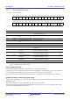
Table Of Contents
- 37. Serial Sound Interface (SSI)
- 38. Serial Peripheral Interface (RSPIa)
- 38.1 Overview
- 38.2 Register Descriptions
- 38.2.1 RSPI Control Register (SPCR)
- 38.2.2 RSPI Slave Select Polarity Register (SSLP)
- 38.2.3 RSPI Pin Control Register (SPPCR)
- 38.2.4 RSPI Status Register (SPSR)
- 38.2.5 RSPI Data Register (SPDR)
- 38.2.6 RSPI Sequence Control Register (SPSCR)
- 38.2.7 RSPI Sequence Status Register (SPSSR)
- 38.2.8 RSPI Bit Rate Register (SPBR)
- 38.2.9 RSPI Data Control Register (SPDCR)
- 38.2.10 RSPI Clock Delay Register (SPCKD)
- 38.2.11 RSPI Slave Select Negation Delay Register (SSLND)
- 38.2.12 RSPI Next-Access Delay Register (SPND)
- 38.2.13 RSPI Control Register 2 (SPCR2)
- 38.2.14 RSPI Command Register m (SPCMDm) (m = 0 to 7)
- 38.3 Operation
- 38.3.1 Overview of RSPI Operations
- 38.3.2 Controlling RSPI Pins
- 38.3.3 RSPI System Configuration Examples
- 38.3.3.1 Single Master/Single Slave (with This MCU Acting as Master)
- 38.3.3.2 Single Master/Single Slave (with This MCU Acting as Slave)
- 38.3.3.3 Single Master/Multi-Slave (with This MCU Acting as Master)
- 38.3.3.4 Single Master/Multi-Slave (with This MCU Acting as Slave)
- 38.3.3.5 Multi-Master/Multi-Slave (with This MCU Acting as Master)
- 38.3.3.6 Master (Clock Synchronous Operation)/Slave (Clock Synchronous Operation) (with This MCU Acting as Master)
- 38.3.3.7 Master (Clock Synchronous Operation)/Slave (Clock Synchronous Operation) (with This MCU Acting as Slave)
- 38.3.4 Data Format
- 38.3.5 Transfer Format
- 38.3.6 Communications Operating Mode
- 38.3.7 Transmit Buffer Empty/Receive Buffer Full Interrupts
- 38.3.8 Error Detection
- 38.3.9 Initializing RSPI
- 38.3.10 SPI Operation
- 38.3.11 Clock Synchronous Operation
- 38.3.12 Loopback Mode
- 38.3.13 Self-Diagnosis of Parity Bit Function
- 38.3.14 Interrupt Sources
- 38.4 Link Operation by Event Linking
- 38.5 Usage Notes
- 39. CRC Calculator (CRC)
- 40. SD Host Interface (SDHIa)
- 40.1 Overview
- 40.2 Register Details
- 40.2.1 Command Register (SDCMD)
- 40.2.2 Argument Register (SDARG)
- 40.2.3 Data Stop Register (SDSTOP)
- 40.2.4 Block Count Register (SDBLKCNT)
- 40.2.5 Response Register 10 (SDRSP10), Response Register 32 (SDRSP32), Response Register 54 (SDRSP54), Response Register 76 (SDRSP76)
- 40.2.6 SD Status Register 1 (SDSTS1)
- 40.2.7 SD Status Register 2 (SDSTS2)
- 40.2.8 SD Interrupt Mask Register 1 (SDIMSK1)
- 40.2.9 SD Interrupt Mask Register 2 (SDIMSK2)
- 40.2.10 SDHI Clock Control Register (SDCLKCR)
- 40.2.11 Transfer Data Size Register (SDSIZE)
- 40.2.12 Card Access Option Register (SDOPT)
- 40.2.13 SD Error Status Register 1 (SDERSTS1)
- 40.2.14 SD Error Status Register 2 (SDERSTS2)
- 40.2.15 SD Buffer Register (SDBUFR)
- 40.2.16 SDIO Mode Control Register (SDIOMD)
- 40.2.17 SDIO Status Register (SDIOSTS)
- 40.2.18 SDIO Interrupt Mask Register (SDIOIMSK)
- 40.2.19 DMA Transfer Enable Register (SDDMAEN)
- 40.2.20 SDHI Software Reset Register (SDRST)
- 40.2.21 Swap Control Register (SDSWAP)
- 40.3 SDHI Operation
- 40.3.1 Data Block Format of the SD Card
- 40.3.2 SD Buffer and the SDBUFR Register
- 40.3.3 SD Card Detection
- 40.3.4 SD Card Write Protection
- 40.3.5 Communication Errors and Timeouts
- 40.3.6 Examples of Issuing a Command
- 40.3.6.1 Command Absent of Response Reception and Data Transfer
- 40.3.6.2 Command Absent of Data Transfer
- 40.3.6.3 Single Block Read Command (CMD17)
- 40.3.6.4 Single Block Write Command (CMD24)
- 40.3.6.5 Multi-Block Read Command (CMD18)
- 40.3.6.6 Multi-Block Write Command (CMD25)
- 40.3.6.7 IO_RW_DIRECT Command (CMD52)
- 40.3.6.8 IO_RW_EXTENDED Command (CMD53 (Multi-Block Read))
- 40.3.6.9 IO_RW_EXTENDED (CMD53 Multi-Block Write)
- 40.3.6.10 DMA Transfer
- 40.4 Interrupts
- 40.5 Notes on Using the SDHI
- 40.5.1 Illegal Read Access During a Multi-Block Read and How To Avoid It
- 40.5.2 SDBUFR Register Illegal Write Error
- 40.5.3 Automatic Control of the SDHI Clock Output
- 40.5.4 Restrictions on Setting the C52PUB Bit During a Multi-Block Write Sequence
- 40.5.5 Note on Setting the SDCLKCR Register
- 40.5.6 Writing to the SDSTOP Register During a Multi-Block Read Sequence
- 40.5.7 Controlling Module Operation
- 41. Bluetooth Low Energy (BLE)
- 42. Trusted Secure IP (TSIP-Lite)
- 43. Capacitive Touch Sensing Unit (CTSU)
- 43.1 Overview
- 43.2 Register Descriptions
- 43.2.1 CTSU Control Register 0 (CTSUCR0)
- 43.2.2 CTSU Control Register 1 (CTSUCR1)
- 43.2.3 CTSU Synchronous Noise Reduction Setting Register (CTSUSDPRS)
- 43.2.4 CTSU Sensor Stabilization Wait Control Register (CTSUSST)
- 43.2.5 CTSU Measurement Channel Register 0 (CTSUMCH0)
- 43.2.6 CTSU Measurement Channel Register 1 (CTSUMCH1)
- 43.2.7 CTSU Channel Enable Control Register 0 (CTSUCHAC0)
- 43.2.8 CTSU Channel Enable Control Register 1 (CTSUCHAC1)
- 43.2.9 CTSU Channel Enable Control Register 2 (CTSUCHAC2)
- 43.2.10 CTSU Channel Enable Control Register 3 (CTSUCHAC3)
- 43.2.11 CTSU Channel Enable Control Register 4 (CTSUCHAC4)
- 43.2.12 CTSU Channel Transmit/Receive Control Register 0 (CTSUCHTRC0)
- 43.2.13 CTSU Channel Transmit/Receive Control Register 1 (CTSUCHTRC1)
- 43.2.14 CTSU Channel Transmit/Receive Control Register 2 (CTSUCHTRC2)
- 43.2.15 CTSU Channel Transmit/Receive Control Register 3 (CTSUCHTRC3)
- 43.2.16 CTSU Channel Transmit/Receive Control Register 4 (CTSUCHTRC4)
- 43.2.17 CTSU High-Pass Noise Reduction Control Register (CTSUDCLKC)
- 43.2.18 CTSU Status Register (CTSUST)
- 43.2.19 CTSU High-Pass Noise Reduction Spectrum Diffusion Control Register (CTSUSSC)
- 43.2.20 CTSU Sensor Offset Register 0 (CTSUSO0)
- 43.2.21 CTSU Sensor Offset Register 1 (CTSUSO1)
- 43.2.22 CTSU Sensor Counter (CTSUSC)
- 43.2.23 CTSU Reference Counter (CTSURC)
- 43.2.24 CTSU Error Status Register (CTSUERRS)
- 43.3 Operation
- 43.4 Usage Notes
- 44. 12-Bit A/D Converter (S12ADE)
- 44.1 Overview
- 44.2 Register Descriptions
- 44.2.1 A/D Data Registers y (ADDRy) (y = 0 to 7, 16 to 20, 27), A/D Data Duplication Register (ADDBLDR), A/D Temperature Sensor Data Register (ADTSDR), A/D Internal Reference Voltage Data Register (ADOCDR)
- 44.2.2 A/D Self-Diagnosis Data Register (ADRD)
- 44.2.3 A/D Control Register (ADCSR)
- 44.2.4 A/D Channel Select Register A0 (ADANSA0)
- 44.2.5 A/D Channel Select Register A1 (ADANSA1)
- 44.2.6 A/D Channel Select Register B0 (ADANSB0)
- 44.2.7 A/D Channel Select Register B1 (ADANSB1)
- 44.2.8 A/D-Converted Value Addition/Average Function Select Register 0 (ADADS0)
- 44.2.9 A/D-Converted Value Addition/Average Function Select Register 1 (ADADS1)
- 44.2.10 A/D-Converted Value Addition/Average Count Select Register (ADADC)
- 44.2.11 A/D Control Extended Register (ADCER)
- 44.2.12 A/D Conversion Start Trigger Select Register (ADSTRGR)
- 44.2.13 A/D Conversion Extended Input Control Register (ADEXICR)
- 44.2.14 A/D Sampling State Register n (ADSSTRn) (n = 0 to 7, L, T, O)
- 44.2.15 A/D Disconnection Detection Control Register (ADDISCR)
- 44.2.16 A/D Event Link Control Register (ADELCCR)
- 44.2.17 A/D Group Scan Priority Control Register (ADGSPCR)
- 44.2.18 A/D Compare Function Control Register (ADCMPCR)
- 44.2.19 A/D Compare Function Window A Channel Select Register 0 (ADCMPANSR0)
- 44.2.20 A/D Compare Function Window A Channel Select Register 1 (ADCMPANSR1)
- 44.2.21 A/D Compare Function Window A Extended Input Select Register (ADCMPANSER)
- 44.2.22 A/D Compare Function Window A Comparison Condition Setting Register 0 (ADCMPLR0)
- 44.2.23 A/D Compare Function Window A Comparison Condition Setting Register 1 (ADCMPLR1)
- 44.2.24 A/D Compare Function Window A Extended Input Comparison Condition Setting Register (ADCMPLER)
- 44.2.25 A/D Compare Function Window A Lower-Side Level Setting Register (ADCMPDR0)
- 44.2.26 A/D Compare Function Window A Upper-Side Level Setting Register (ADCMPDR1)
- 44.2.27 A/D Compare Function Window A Channel Status Register 0 (ADCMPSR0)
- 44.2.28 A/D Compare Function Window A Channel Status Register 1 (ADCMPSR1)
- 44.2.29 A/D Compare Function Window A Extended Input Channel Status Register (ADCMPSER)
- 44.2.30 A/D High-Potential/Low-Potential Reference Voltage Control Register (ADHVREFCNT)
- 44.2.31 A/D Compare Function Window A/B Status Monitor Register (ADWINMON)
- 44.2.32 A/D Compare Function Window B Channel Select Register (ADCMPBNSR)
- 44.2.33 A/D Compare Function Window B Lower-Side Level Setting Register (ADWINLLB)
- 44.2.34 A/D Compare Function Window B Upper-Side Level Setting Register (ADWINULB)
- 44.2.35 A/D Compare Function Window B Channel Status Register (ADCMPBSR)
- 44.2.36 A/D Data Storage Buffer Register n (ADBUFn) (n = 0 to 15)

R01UH0823EJ0110 Rev.1.10 Page 1313 of 1852
Nov 30, 2020
RX23W Group 37. Serial Sound Interface (SSI)
Note 1. While this module is muted, low is transmitted regardless of the value of serial data, but data transmission is not stopped. Since
the number of data in the transmit FIFO decreases, write dummy data to the SSIFTDR register to prevent the generation of a
transmit underflow. When the MUEN bit is set to 1, the SSITXD0 pin immediately becomes low without synchronizing SSIWS0
pin.
Note 2. Set the SCKD and SWSD bits to the same value. Other settings are prohibited.
Note 3. Rewriting is allowed only in the idle state.
b12 SWSP Word Select Polarity 0: SSIWS0 is low for the 1st system word, high for the 2nd
system word.
1: SSIWS0 is high for the 1st system word, low for the 2nd
system word.
R/W
b13 SCKP Serial Bit Clock Polarity*
3
0: SSIWS0 and SSITXD0 change at the SSISCK0 falling edge
(SSIWS0 and SSIRXD0 are sampled at the SSISCK0 rising
edge).
1: SSIWS0 and SSITXD0 change at the SSISCK0 rising edge
(SSIWS0 and SSITXD0 are sampled at the SSISCK0 falling
edge).
R/W
b14 SWSD Word Select Direction*
2,
*
3
0: SSIWS0 pin is input (slave mode).
1: SSIWS0 pin is output (master mode).
R/W
b15 SCKD Serial Bit Clock Direction*
2,
*
3
0: SSISCK0 pin is input (slave mode).
1: SSISCK0 pin is output (master mode).
R/W
b18 to b16 SWL[2:0] System Word Length*
3
Set the system word length to the bit clock frequency/2 fs.
b18 b16
0 0 0: 8 bits (serial bit clock frequency = 16 fs)
0 0 1: 6 bits (serial bit clock frequency = 32 fs)
0 1 0: 24 bits (serial bit clock frequency = 48 fs)
0 1 1: 32 bits (serial bit clock frequency = 64 fs)
Settings other than above are prohibited.
R/W
b21 to b19 DWL[2:0] Data Word Length*
3
b21 b19
000:8 bits
0 0 1: 16 bits
0 1 0: 18 bits
0 1 1: 20 bits
1 0 0: 22 bits
1 0 1: 24 bits
Settings other than above are prohibited.
R/W
b23, b22 CHNL[1:0] Channels*
3
b23 b22
0 0: One channel
Settings other than above are prohibited.
R/W
b24 — Reserved This bit is read as 0. The write value should be 0. R/W
b25 IIEN Idle Interrupt Enable 0: Disables an idle interrupt.
1: Enables an idle interrupt.
R/W
b26 ROIEN Receive Overflow Interrupt
Enable
0: Disables a receive overflow interrupt.
1: Enables a receive overflow interrupt.
R/W
b27 RUIEN Receive Underflow Interrupt
Enable
0: Disables a receive underflow interrupt.
1: Enables a receive underflow interrupt.
R/W
b28 TOIEN Transmit Overflow Interrupt
Enable
0: Disables a transmit overflow interrupt.
1: Enables a transmit overflow interrupt.
R/W
b29 TUIEN Transmit Underflow Interrupt
Enable
0: Disables a transmit underflow interrupt.
1: Enables a transmit underflow interrupt.
R/W
b30 CKS Audio Clock Select*
3
0: AUDIO_MCLK input
1: Main clock
R/W
b31 — Reserved This bit is read as 0. The write value should be 0. R/W
Bit Symbol Bit Name Description R/W