
Users Manual
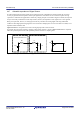
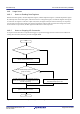
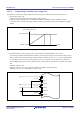
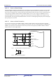
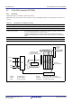
Table Of Contents
- 45. 12-Bit D/A Converter (R12DAA)
- 46. Temperature Sensor (TEMPSA)
- 47. Comparator B (CMPBa)
- 47.1 Overview
- 47.2 Register Descriptions
- 47.2.1 Comparator B1 Control Register 1 (CPB1CNT1)
- 47.2.2 Comparator B1 Control Register 2 (CPB1CNT2)
- 47.2.3 Comparator B1 Flag Register (CPB1FLG)
- 47.2.4 Comparator B1 Interrupt Control Register (CPB1INT)
- 47.2.5 Comparator B1 Filter Select Register (CPB1F)
- 47.2.6 Comparator B1 Mode Select Register (CPB1MD)
- 47.2.7 Comparator B1 Reference Input Voltage Select Register (CPB1REF)
- 47.2.8 Comparator B1 Output Control Register (CPB1OCR)
- 47.3 Operation
- 47.4 Comparator B2 and Comparator B3 Interrupts
- 47.5 Usage Note
- 48. Data Operation Circuit (DOC)
- 49. RAM
- 50. Flash Memory (FLASH)
- 50.1 Overview
- 50.2 ROM Area and Block Configuration
- 50.3 E2 DataFlash Area and Block Configuration
- 50.4 Register Descriptions
- 50.4.1 E2 DataFlash Control Register (DFLCTL)
- 50.4.2 Flash P/E Mode Entry Register (FENTRYR)
- 50.4.3 Protection Unlock Register (FPR)
- 50.4.4 Protection Unlock Status Register (FPSR)
- 50.4.5 Flash P/E Mode Control Register (FPMCR)
- 50.4.6 Flash Initial Setting Register (FISR)
- 50.4.7 Flash Reset Register (FRESETR)
- 50.4.8 Flash Area Select Register (FASR)
- 50.4.9 Flash Control Register (FCR)
- 50.4.10 Flash Extra Area Control Register (FEXCR)
- 50.4.11 Flash Processing Start Address Register H (FSARH)
- 50.4.12 Flash Processing Start Address Register L (FSARL)
- 50.4.13 Flash Processing End Address Register H (FEARH)
- 50.4.14 Flash Processing End Address Register L (FEARL)
- 50.4.15 Flash Write Buffer Register n (FWBn) (n = 0 to 3)
- 50.4.16 Flash Status Register 0 (FSTATR0)
- 50.4.17 Flash Status Register 1 (FSTATR1)
- 50.4.18 Flash Error Address Monitor Register H (FEAMH)
- 50.4.19 Flash Error Address Monitor Register L (FEAML)
- 50.4.20 Flash Start-Up Setting Monitor Register (FSCMR)
- 50.4.21 Flash Access Window Start Address Monitor Register (FAWSMR)
- 50.4.22 Flash Access Window End Address Monitor Register (FAWEMR)
- 50.4.23 Unique ID Register n (UIDRn) (n = 0 to 3)
- 50.5 Start-Up Program Protection
- 50.6 Area Protection
- 50.7 Programming and Erasure
- 50.8 Boot Mode
- 50.9 Flash Memory Protection
- 50.10 Communication Protocol
- 50.10.1 State Transition in Boot Mode (SCI Interface)
- 50.10.2 Command and Response Configuration
- 50.10.3 Response to Undefined Commands
- 50.10.4 Boot Mode Status Inquiry
- 50.10.5 Inquiry Commands
- 50.10.6 Setting Commands
- 50.10.7 ID Code Authentication Command
- 50.10.8 Program/Erase Commands
- 50.10.9 Read-Check Commands
- 50.11 Serial Programmer Operation in Boot Mode (SCI Interface)
- 50.11.1 Bit Rate Automatic Adjustment Procedure
- 50.11.2 Procedure to Receive the MCU Information
- 50.11.3 Procedure to Select the Device and Change the Bit Rate
- 50.11.4 Procedure for Transition to the Program/Erase Host Command Wait State
- 50.11.5 Procedure to Unlock Boot Mode ID Code Protection
- 50.11.6 Procedure to Erase the User Area and Data Area
- 50.11.7 Procedure to Program the User Area and Data Area
- 50.11.8 Procedure to Check Data in the User Area
- 50.11.9 Procedure to Check Data in the Data Area
- 50.11.10 Procedure to Set the Access Window in the User Area
- 50.12 Rewriting by Self-Programming
- 50.13 Usage Notes
- 50.14 Usage Notes in Boot Mode
- 51. Electrical Characteristics
- 51.1 Absolute Maximum Ratings
- 51.2 DC Characteristics
- 51.3 AC Characteristics
- 51.3.1 Clock Timing
- 51.3.2 Reset Timing
- 51.3.3 Timing of Recovery from Low Power Consumption Modes
- 51.3.4 Control Signal Timing
- 51.3.5 Timing of On-Chip Peripheral Modules
- 51.3.5.1 Timing of I/O Ports
- 51.3.5.2 Timing of MTU/TPU
- 51.3.5.3 Timing of POE
- 51.3.5.4 Timing of TMR
- 51.3.5.5 Timing of SCI
- 51.3.5.6 Timing of RIIC
- 51.3.5.7 Timing of RSPI
- 51.3.5.8 Timing of SSI
- 51.3.5.9 Timing of SDHI
- 51.3.5.10 Timing of A/D Converter Trigger
- 51.3.5.11 Timing of CAC
- 51.3.5.12 Timing of CLKOUT
- 51.3.5.13 Timing of CLKOUT_RF
- 51.4 USB Characteristics
- 51.5 A/D Conversion Characteristics
- 51.6 D/A Conversion Characteristics
- 51.7 Temperature Sensor Characteristics
- 51.8 Comparator Characteristics
- 51.9 CTSU Characteristics
- 51.10 Characteristics of Power-On Reset Circuit and Voltage Detection Circuit
- 51.11 Oscillation Stop Detection Timing
- 51.12 Battery Backup Function Characteristics
- 51.13 ROM (Flash Memory for Code Storage) Characteristics
- 51.14 E2 DataFlash Characteristics (Flash Memory for Data Storage)
- 51.15 BLE Characteristics
- 51.16 Usage Notes
- Appendix 1. Port States in Each Processing Mode
- Appendix 2. Package Dimensions
- REVISION HISTORY
- Colophon
- Address List
- Back cover

R01UH0823EJ0110 Rev.1.10 Page 1634 of 1852
Nov 30, 2020
RX23W Group 44. 12-Bit A/D Converter (S12ADE)
44.8.3 A/D Conversion Restarting Timing and Termination Timing
It takes a maximum of six ADCLK cycles for the idle analog unit of the 12-bit A/D converter to be restarted by setting
the ADCSR.ADST bit to 1. It takes a maximum of three ADCLK cycles for the operating analog unit of the 12-bit A/D
converter to be terminated by setting the ADCSR.ADST bit to 0.
44.8.4 Notes on Scan End Interrupt Handling
When scanning the same analog input twice using any trigger, the first A/D-converted data is overwritten with the second
A/D-converted data in the case that the CPU does not complete reading the A/D-converted data by the time the A/D
conversion of the first analog input for the second scan ends after the first scan end interrupt is generated.
44.8.5 Module Stop Function Setting
Operation of the 12-bit A/D converter can be disabled or enabled by setting module stop control register A (MSTPCRA).
The initial setting is for operation of the 12-bit A/D converter to be halted. Register access is enabled by releasing the
module stop state.
After the module stop state is released, wait for 1 µs to start A/D conversion. For details, refer to
section 11, Low
Power Consumption
.
44.8.6 Notes on Entering Low Power Consumption States
Before entering the module stop state or software standby mode, make sure to stop A/D conversion. Here, set the
ADCSR.ADST bit to 0, and secure certain period of time until the analog unit of the 12-bit A/D converter is stopped.
Follow the procedure given below to secure this time.
Follow the procedure for clear operation by software through the ADCSR.ADST bit, shown in
Figure 44.29. After that,
wait for two clock cycles of ADCLK before entering the peripheral module stop state or software standby mode.
44.8.7 Notes on Canceling Software Standby Mode
After software standby mode is canceled, wait until the crystal oscillation stabilization time or the PLL circuit
stabilization time elapses, and then wait for 1 µs before starting A/D conversion. For details, refer to
section 11, Low
Power Consumption
.
44.8.8 Pin Setting when the 12-bit A/D Converter is Used
When the 12-bit A/D converter is used, do not set any pin of port 4 as output.
Output from any of the pins may affect on A/D conversion accuracy because analog power supply is used in the part of
the port 4 circuit.
44.8.9 Error in Absolute Accuracy When Disconnection Detection Assistance is in Use
Using disconnection detection assistance leads to an error in absolute accuracy of the A/D converter. This is because an
error voltage is input to the analog input pins due to the resistive voltage division between the pull-up or pull-down
resistor (Rp) and the resistance of the signal source (Rs). This error in absolute accuracy is calculated from the following
formula. Only use disconnection detection assistance after thorough evaluation.
Maximum error in absolute accuracy (LSB) = 4095 × Rs / Rp