
Users Manual
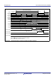
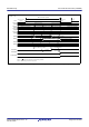
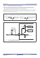
Table Of Contents
- 45. 12-Bit D/A Converter (R12DAA)
- 46. Temperature Sensor (TEMPSA)
- 47. Comparator B (CMPBa)
- 47.1 Overview
- 47.2 Register Descriptions
- 47.2.1 Comparator B1 Control Register 1 (CPB1CNT1)
- 47.2.2 Comparator B1 Control Register 2 (CPB1CNT2)
- 47.2.3 Comparator B1 Flag Register (CPB1FLG)
- 47.2.4 Comparator B1 Interrupt Control Register (CPB1INT)
- 47.2.5 Comparator B1 Filter Select Register (CPB1F)
- 47.2.6 Comparator B1 Mode Select Register (CPB1MD)
- 47.2.7 Comparator B1 Reference Input Voltage Select Register (CPB1REF)
- 47.2.8 Comparator B1 Output Control Register (CPB1OCR)
- 47.3 Operation
- 47.4 Comparator B2 and Comparator B3 Interrupts
- 47.5 Usage Note
- 48. Data Operation Circuit (DOC)
- 49. RAM
- 50. Flash Memory (FLASH)
- 50.1 Overview
- 50.2 ROM Area and Block Configuration
- 50.3 E2 DataFlash Area and Block Configuration
- 50.4 Register Descriptions
- 50.4.1 E2 DataFlash Control Register (DFLCTL)
- 50.4.2 Flash P/E Mode Entry Register (FENTRYR)
- 50.4.3 Protection Unlock Register (FPR)
- 50.4.4 Protection Unlock Status Register (FPSR)
- 50.4.5 Flash P/E Mode Control Register (FPMCR)
- 50.4.6 Flash Initial Setting Register (FISR)
- 50.4.7 Flash Reset Register (FRESETR)
- 50.4.8 Flash Area Select Register (FASR)
- 50.4.9 Flash Control Register (FCR)
- 50.4.10 Flash Extra Area Control Register (FEXCR)
- 50.4.11 Flash Processing Start Address Register H (FSARH)
- 50.4.12 Flash Processing Start Address Register L (FSARL)
- 50.4.13 Flash Processing End Address Register H (FEARH)
- 50.4.14 Flash Processing End Address Register L (FEARL)
- 50.4.15 Flash Write Buffer Register n (FWBn) (n = 0 to 3)
- 50.4.16 Flash Status Register 0 (FSTATR0)
- 50.4.17 Flash Status Register 1 (FSTATR1)
- 50.4.18 Flash Error Address Monitor Register H (FEAMH)
- 50.4.19 Flash Error Address Monitor Register L (FEAML)
- 50.4.20 Flash Start-Up Setting Monitor Register (FSCMR)
- 50.4.21 Flash Access Window Start Address Monitor Register (FAWSMR)
- 50.4.22 Flash Access Window End Address Monitor Register (FAWEMR)
- 50.4.23 Unique ID Register n (UIDRn) (n = 0 to 3)
- 50.5 Start-Up Program Protection
- 50.6 Area Protection
- 50.7 Programming and Erasure
- 50.8 Boot Mode
- 50.9 Flash Memory Protection
- 50.10 Communication Protocol
- 50.10.1 State Transition in Boot Mode (SCI Interface)
- 50.10.2 Command and Response Configuration
- 50.10.3 Response to Undefined Commands
- 50.10.4 Boot Mode Status Inquiry
- 50.10.5 Inquiry Commands
- 50.10.6 Setting Commands
- 50.10.7 ID Code Authentication Command
- 50.10.8 Program/Erase Commands
- 50.10.9 Read-Check Commands
- 50.11 Serial Programmer Operation in Boot Mode (SCI Interface)
- 50.11.1 Bit Rate Automatic Adjustment Procedure
- 50.11.2 Procedure to Receive the MCU Information
- 50.11.3 Procedure to Select the Device and Change the Bit Rate
- 50.11.4 Procedure for Transition to the Program/Erase Host Command Wait State
- 50.11.5 Procedure to Unlock Boot Mode ID Code Protection
- 50.11.6 Procedure to Erase the User Area and Data Area
- 50.11.7 Procedure to Program the User Area and Data Area
- 50.11.8 Procedure to Check Data in the User Area
- 50.11.9 Procedure to Check Data in the Data Area
- 50.11.10 Procedure to Set the Access Window in the User Area
- 50.12 Rewriting by Self-Programming
- 50.13 Usage Notes
- 50.14 Usage Notes in Boot Mode
- 51. Electrical Characteristics
- 51.1 Absolute Maximum Ratings
- 51.2 DC Characteristics
- 51.3 AC Characteristics
- 51.3.1 Clock Timing
- 51.3.2 Reset Timing
- 51.3.3 Timing of Recovery from Low Power Consumption Modes
- 51.3.4 Control Signal Timing
- 51.3.5 Timing of On-Chip Peripheral Modules
- 51.3.5.1 Timing of I/O Ports
- 51.3.5.2 Timing of MTU/TPU
- 51.3.5.3 Timing of POE
- 51.3.5.4 Timing of TMR
- 51.3.5.5 Timing of SCI
- 51.3.5.6 Timing of RIIC
- 51.3.5.7 Timing of RSPI
- 51.3.5.8 Timing of SSI
- 51.3.5.9 Timing of SDHI
- 51.3.5.10 Timing of A/D Converter Trigger
- 51.3.5.11 Timing of CAC
- 51.3.5.12 Timing of CLKOUT
- 51.3.5.13 Timing of CLKOUT_RF
- 51.4 USB Characteristics
- 51.5 A/D Conversion Characteristics
- 51.6 D/A Conversion Characteristics
- 51.7 Temperature Sensor Characteristics
- 51.8 Comparator Characteristics
- 51.9 CTSU Characteristics
- 51.10 Characteristics of Power-On Reset Circuit and Voltage Detection Circuit
- 51.11 Oscillation Stop Detection Timing
- 51.12 Battery Backup Function Characteristics
- 51.13 ROM (Flash Memory for Code Storage) Characteristics
- 51.14 E2 DataFlash Characteristics (Flash Memory for Data Storage)
- 51.15 BLE Characteristics
- 51.16 Usage Notes
- Appendix 1. Port States in Each Processing Mode
- Appendix 2. Package Dimensions
- REVISION HISTORY
- Colophon
- Address List
- Back cover

R01UH0823EJ0110 Rev.1.10 Page 1626 of 1852
Nov 30, 2020
RX23W Group 44. 12-Bit A/D Converter (S12ADE)
Table 44.10 Times for Conversion during Scanning (in Numbers of Cycles of ADCLK and PCLK)
Note 1. For t
D
, t
DIAG
, t
CONV
, and t
ED
, see Figure 44.22 and Figure 44.23.
Note 2. This is the maximum time required from software writing or trigger input to A/D conversion start.
Note 3. The value is fixed to 0Fh (15 ADCLK) when the temperature sensor output or internal reference voltage is A/D-converted.
Note 4. The required sampling time (ns) is specified according to the voltage conditions. See section 51.5, A/D Conversion
Characteristics.
Note 5. This does not include the time consumed in the path from timer output to trigger input.
Note 6. 2 PCLK + 3 ADCLK when ADCLK is faster than PCLK (PCLK to ADCLK frequency ratio = 1:2 or 1:4).
Figure 44.22 Scan Conversion Timing (Activated by Software or Synchronous Trigger)
Item Symbol
Type/Conditions
UnitSynchronous Trigger
*5
Asynchronous
Trigger
Software
Trigger
Scan start
processing
time*
1,
*
2
A/D
conversion on
group A under
group-A
priority
control.
Group B is to be stopped.
(Group A is activated after
group B is stopped due to
an A/D conversion source
of group A.)
t
D
3 PCLK + 6 ADCLK — — Cycle
Group B is not to be
stopped. (Activation by an
A/D conversion source of
group A.)
2 PCLK + 4 ADCLK — —
A/D
conversion
when self-
diagnosis is
enabled
A/D conversion for self-
diagnosis is to be started.
2 PCLK + 6 ADCLK 4 PCLKB +
6 ADCLK
6 ADCLK
Other than above 2 PCLK + 4 ADCLK 4 PCLKB +
4 ADCLK
4 ADCLK
Disconnection detection assistance processing time t
DIS
The setting of ADNDIS[3:0] (initial value = 00h) × ADCLK*
3
Self-diagnosis
conversion
processing
time*
1
Sampling time t
DIAG
t
SPL
The setting of ADSSTR0 (initial value = 0Dh) × ADCLK*
4
Time for
conversion by
successive
approximation
12-bit conversion accuracy t
SAM
32 ADCLK (during high-speed conversion operation)
41 ADCLK (during low-current conversion operation)
Normal A/D conversion is to be started after
completion of self-diagnosis conversion.
t
DED
2 ADCLK
A/D conversion for self-diagnosis is to be
started after completion of conversion for
continuous scan on the last channel
specified.
t
DSD
2 ADCLK
A/D
conversion
processing
time*
1
Sampling time t
CONV
t
SPL
The setting of ADSSTRn (n = 0 to 7, L, T, O) (initial value =
0Dh) × ADCLK*
4
Time for
conversion by
successive
approximation
12-bit conversion accuracy t
SAM
32 ADCLK (during high-speed conversion operation)
41 ADCLK (during low-current conversion operation)
Scan end processing time*
1
t
ED
1 PCLKB + 3 ADCLK*
6
t
DIAG
t
SCAN
t
CONV
t
ED
DIAG conversion A/D conversion
End
processing
t
D
Software trigger
Synchronous trigger
Waiting
ADST bit
A/D converter