
Users Manual
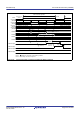
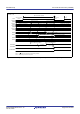
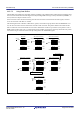
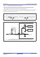
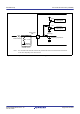
Table Of Contents
- 45. 12-Bit D/A Converter (R12DAA)
- 46. Temperature Sensor (TEMPSA)
- 47. Comparator B (CMPBa)
- 47.1 Overview
- 47.2 Register Descriptions
- 47.2.1 Comparator B1 Control Register 1 (CPB1CNT1)
- 47.2.2 Comparator B1 Control Register 2 (CPB1CNT2)
- 47.2.3 Comparator B1 Flag Register (CPB1FLG)
- 47.2.4 Comparator B1 Interrupt Control Register (CPB1INT)
- 47.2.5 Comparator B1 Filter Select Register (CPB1F)
- 47.2.6 Comparator B1 Mode Select Register (CPB1MD)
- 47.2.7 Comparator B1 Reference Input Voltage Select Register (CPB1REF)
- 47.2.8 Comparator B1 Output Control Register (CPB1OCR)
- 47.3 Operation
- 47.4 Comparator B2 and Comparator B3 Interrupts
- 47.5 Usage Note
- 48. Data Operation Circuit (DOC)
- 49. RAM
- 50. Flash Memory (FLASH)
- 50.1 Overview
- 50.2 ROM Area and Block Configuration
- 50.3 E2 DataFlash Area and Block Configuration
- 50.4 Register Descriptions
- 50.4.1 E2 DataFlash Control Register (DFLCTL)
- 50.4.2 Flash P/E Mode Entry Register (FENTRYR)
- 50.4.3 Protection Unlock Register (FPR)
- 50.4.4 Protection Unlock Status Register (FPSR)
- 50.4.5 Flash P/E Mode Control Register (FPMCR)
- 50.4.6 Flash Initial Setting Register (FISR)
- 50.4.7 Flash Reset Register (FRESETR)
- 50.4.8 Flash Area Select Register (FASR)
- 50.4.9 Flash Control Register (FCR)
- 50.4.10 Flash Extra Area Control Register (FEXCR)
- 50.4.11 Flash Processing Start Address Register H (FSARH)
- 50.4.12 Flash Processing Start Address Register L (FSARL)
- 50.4.13 Flash Processing End Address Register H (FEARH)
- 50.4.14 Flash Processing End Address Register L (FEARL)
- 50.4.15 Flash Write Buffer Register n (FWBn) (n = 0 to 3)
- 50.4.16 Flash Status Register 0 (FSTATR0)
- 50.4.17 Flash Status Register 1 (FSTATR1)
- 50.4.18 Flash Error Address Monitor Register H (FEAMH)
- 50.4.19 Flash Error Address Monitor Register L (FEAML)
- 50.4.20 Flash Start-Up Setting Monitor Register (FSCMR)
- 50.4.21 Flash Access Window Start Address Monitor Register (FAWSMR)
- 50.4.22 Flash Access Window End Address Monitor Register (FAWEMR)
- 50.4.23 Unique ID Register n (UIDRn) (n = 0 to 3)
- 50.5 Start-Up Program Protection
- 50.6 Area Protection
- 50.7 Programming and Erasure
- 50.8 Boot Mode
- 50.9 Flash Memory Protection
- 50.10 Communication Protocol
- 50.10.1 State Transition in Boot Mode (SCI Interface)
- 50.10.2 Command and Response Configuration
- 50.10.3 Response to Undefined Commands
- 50.10.4 Boot Mode Status Inquiry
- 50.10.5 Inquiry Commands
- 50.10.6 Setting Commands
- 50.10.7 ID Code Authentication Command
- 50.10.8 Program/Erase Commands
- 50.10.9 Read-Check Commands
- 50.11 Serial Programmer Operation in Boot Mode (SCI Interface)
- 50.11.1 Bit Rate Automatic Adjustment Procedure
- 50.11.2 Procedure to Receive the MCU Information
- 50.11.3 Procedure to Select the Device and Change the Bit Rate
- 50.11.4 Procedure for Transition to the Program/Erase Host Command Wait State
- 50.11.5 Procedure to Unlock Boot Mode ID Code Protection
- 50.11.6 Procedure to Erase the User Area and Data Area
- 50.11.7 Procedure to Program the User Area and Data Area
- 50.11.8 Procedure to Check Data in the User Area
- 50.11.9 Procedure to Check Data in the Data Area
- 50.11.10 Procedure to Set the Access Window in the User Area
- 50.12 Rewriting by Self-Programming
- 50.13 Usage Notes
- 50.14 Usage Notes in Boot Mode
- 51. Electrical Characteristics
- 51.1 Absolute Maximum Ratings
- 51.2 DC Characteristics
- 51.3 AC Characteristics
- 51.3.1 Clock Timing
- 51.3.2 Reset Timing
- 51.3.3 Timing of Recovery from Low Power Consumption Modes
- 51.3.4 Control Signal Timing
- 51.3.5 Timing of On-Chip Peripheral Modules
- 51.3.5.1 Timing of I/O Ports
- 51.3.5.2 Timing of MTU/TPU
- 51.3.5.3 Timing of POE
- 51.3.5.4 Timing of TMR
- 51.3.5.5 Timing of SCI
- 51.3.5.6 Timing of RIIC
- 51.3.5.7 Timing of RSPI
- 51.3.5.8 Timing of SSI
- 51.3.5.9 Timing of SDHI
- 51.3.5.10 Timing of A/D Converter Trigger
- 51.3.5.11 Timing of CAC
- 51.3.5.12 Timing of CLKOUT
- 51.3.5.13 Timing of CLKOUT_RF
- 51.4 USB Characteristics
- 51.5 A/D Conversion Characteristics
- 51.6 D/A Conversion Characteristics
- 51.7 Temperature Sensor Characteristics
- 51.8 Comparator Characteristics
- 51.9 CTSU Characteristics
- 51.10 Characteristics of Power-On Reset Circuit and Voltage Detection Circuit
- 51.11 Oscillation Stop Detection Timing
- 51.12 Battery Backup Function Characteristics
- 51.13 ROM (Flash Memory for Code Storage) Characteristics
- 51.14 E2 DataFlash Characteristics (Flash Memory for Data Storage)
- 51.15 BLE Characteristics
- 51.16 Usage Notes
- Appendix 1. Port States in Each Processing Mode
- Appendix 2. Package Dimensions
- REVISION HISTORY
- Colophon
- Address List
- Back cover

R01UH0823EJ0110 Rev.1.10 Page 1625 of 1852
Nov 30, 2020
RX23W Group 44. 12-Bit A/D Converter (S12ADE)
44.3.5.4 Restrictions for Compare Function
The following restrictions are provided for the compare function.
1. The compare function must not be used together the self-diagnosis function or double trigger mode. (The compare
function is not available for the ADRD register and the ADDBLDR register.)
2. Specify single scan mode when using match/mismatch event outputs.
3. When temperature sensor or internal reference voltage is selected for window A, window B operations are disabled.
4. When temperature sensor or internal reference voltage is selected for window B, window A operations are disabled.
5. It is prohibited to set the same channel for window A and window B.
6. When using the buffer function, specify single scan mode. (It is also prohibited to use double trigger mode
together.)
7. Set the reference voltage values so that the high-side reference voltage value is equal to or larger than the low-side
reference voltage value.
44.3.6 Analog Input Sampling Time and Scan Conversion Time
Scan conversion can be activated either by software, synchronous trigger, or asynchronous trigger input. After the start-
of-scanning-delay time (t
D
) has elapsed, processing for disconnection detection assistance and processing of conversion
for self-diagnosis proceed, and this is followed by processing for A/D conversion.
Figure 44.22 shows the scan conversion timing in single scan mode, in which scan conversion is activated by software
or a synchronous trigger.
Figure 44.23 shows the scan conversion timing in single scan mode, in which scan conversion
is activated by an asynchronous trigger. The scan conversion time (t
SCAN
) includes the start-of-scanning-delay time (t
D
),
disconnection detection assistance processing time (t
DIS
)*
1
, self-diagnosis A/D conversion processing time (t
DIAG
)*
2
, A/
D conversion processing time (t
CONV
), and end-of-scanning-delay time (t
ED
).
The A/D conversion processing time (t
CONV
) consists of sampling time (t
SPL
) and time for conversion by successive
approximation (t
SAM
). The sampling time (t
SPL
) is used to charge sample-and-hold circuits in the A/D converter. If there
is not sufficient sampling time due to the high impedance of an analog input signal source, or if the A/D conversion clock
(ADCLK) is slow, sampling time can be adjusted using the ADSSTRn register.
The time for conversion by successive approximation (t
SAM
) is at 32 ADCLK states during high-speed conversion
operation, and 41 ADCLK states during low-current conversion operation.
Table 44.10 shows the scan conversion time.
The scan conversion time (t
SCAN
) in single scan mode for which the number of selected channels is n can be determined
as follows:
t
SCAN
= t
D
+ (t
DIS
× n) + t
DIAG
+ (t
CONV
× n)*
3
+ t
ED
The scan conversion time for the first cycle in continuous scan mode is t
SCAN
for single scan minus t
ED
.
The scan conversion time for the second and subsequent cycles in continuous scan mode is fixed to (t
DIS
× n) + t
DIAG
+
t
DSD
+ (t
CONV
× n).
Note 1. When disconnection detection assistance is not selected, t
DIS
= 0. The auto-discharge period of 15 ADCLK
states is inserted only when the temperature sensor or internal reference voltage is A/D-converted.
Note 2. When the self-diagnosis function is not used, t
DIAG
= 0, t
DSD
= 0.
Note 3. t
CONV
× n when the sampling time (t
SPL
) of selected channels is the same, but it is the total of the sampling time
of each channel and time for conversion by successive approximation (t
SAM
).