
Users Manual
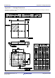
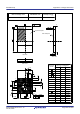
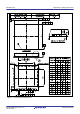
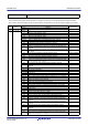
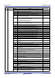
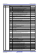
Table Of Contents
- 45. 12-Bit D/A Converter (R12DAA)
- 46. Temperature Sensor (TEMPSA)
- 47. Comparator B (CMPBa)
- 47.1 Overview
- 47.2 Register Descriptions
- 47.2.1 Comparator B1 Control Register 1 (CPB1CNT1)
- 47.2.2 Comparator B1 Control Register 2 (CPB1CNT2)
- 47.2.3 Comparator B1 Flag Register (CPB1FLG)
- 47.2.4 Comparator B1 Interrupt Control Register (CPB1INT)
- 47.2.5 Comparator B1 Filter Select Register (CPB1F)
- 47.2.6 Comparator B1 Mode Select Register (CPB1MD)
- 47.2.7 Comparator B1 Reference Input Voltage Select Register (CPB1REF)
- 47.2.8 Comparator B1 Output Control Register (CPB1OCR)
- 47.3 Operation
- 47.4 Comparator B2 and Comparator B3 Interrupts
- 47.5 Usage Note
- 48. Data Operation Circuit (DOC)
- 49. RAM
- 50. Flash Memory (FLASH)
- 50.1 Overview
- 50.2 ROM Area and Block Configuration
- 50.3 E2 DataFlash Area and Block Configuration
- 50.4 Register Descriptions
- 50.4.1 E2 DataFlash Control Register (DFLCTL)
- 50.4.2 Flash P/E Mode Entry Register (FENTRYR)
- 50.4.3 Protection Unlock Register (FPR)
- 50.4.4 Protection Unlock Status Register (FPSR)
- 50.4.5 Flash P/E Mode Control Register (FPMCR)
- 50.4.6 Flash Initial Setting Register (FISR)
- 50.4.7 Flash Reset Register (FRESETR)
- 50.4.8 Flash Area Select Register (FASR)
- 50.4.9 Flash Control Register (FCR)
- 50.4.10 Flash Extra Area Control Register (FEXCR)
- 50.4.11 Flash Processing Start Address Register H (FSARH)
- 50.4.12 Flash Processing Start Address Register L (FSARL)
- 50.4.13 Flash Processing End Address Register H (FEARH)
- 50.4.14 Flash Processing End Address Register L (FEARL)
- 50.4.15 Flash Write Buffer Register n (FWBn) (n = 0 to 3)
- 50.4.16 Flash Status Register 0 (FSTATR0)
- 50.4.17 Flash Status Register 1 (FSTATR1)
- 50.4.18 Flash Error Address Monitor Register H (FEAMH)
- 50.4.19 Flash Error Address Monitor Register L (FEAML)
- 50.4.20 Flash Start-Up Setting Monitor Register (FSCMR)
- 50.4.21 Flash Access Window Start Address Monitor Register (FAWSMR)
- 50.4.22 Flash Access Window End Address Monitor Register (FAWEMR)
- 50.4.23 Unique ID Register n (UIDRn) (n = 0 to 3)
- 50.5 Start-Up Program Protection
- 50.6 Area Protection
- 50.7 Programming and Erasure
- 50.8 Boot Mode
- 50.9 Flash Memory Protection
- 50.10 Communication Protocol
- 50.10.1 State Transition in Boot Mode (SCI Interface)
- 50.10.2 Command and Response Configuration
- 50.10.3 Response to Undefined Commands
- 50.10.4 Boot Mode Status Inquiry
- 50.10.5 Inquiry Commands
- 50.10.6 Setting Commands
- 50.10.7 ID Code Authentication Command
- 50.10.8 Program/Erase Commands
- 50.10.9 Read-Check Commands
- 50.11 Serial Programmer Operation in Boot Mode (SCI Interface)
- 50.11.1 Bit Rate Automatic Adjustment Procedure
- 50.11.2 Procedure to Receive the MCU Information
- 50.11.3 Procedure to Select the Device and Change the Bit Rate
- 50.11.4 Procedure for Transition to the Program/Erase Host Command Wait State
- 50.11.5 Procedure to Unlock Boot Mode ID Code Protection
- 50.11.6 Procedure to Erase the User Area and Data Area
- 50.11.7 Procedure to Program the User Area and Data Area
- 50.11.8 Procedure to Check Data in the User Area
- 50.11.9 Procedure to Check Data in the Data Area
- 50.11.10 Procedure to Set the Access Window in the User Area
- 50.12 Rewriting by Self-Programming
- 50.13 Usage Notes
- 50.14 Usage Notes in Boot Mode
- 51. Electrical Characteristics
- 51.1 Absolute Maximum Ratings
- 51.2 DC Characteristics
- 51.3 AC Characteristics
- 51.3.1 Clock Timing
- 51.3.2 Reset Timing
- 51.3.3 Timing of Recovery from Low Power Consumption Modes
- 51.3.4 Control Signal Timing
- 51.3.5 Timing of On-Chip Peripheral Modules
- 51.3.5.1 Timing of I/O Ports
- 51.3.5.2 Timing of MTU/TPU
- 51.3.5.3 Timing of POE
- 51.3.5.4 Timing of TMR
- 51.3.5.5 Timing of SCI
- 51.3.5.6 Timing of RIIC
- 51.3.5.7 Timing of RSPI
- 51.3.5.8 Timing of SSI
- 51.3.5.9 Timing of SDHI
- 51.3.5.10 Timing of A/D Converter Trigger
- 51.3.5.11 Timing of CAC
- 51.3.5.12 Timing of CLKOUT
- 51.3.5.13 Timing of CLKOUT_RF
- 51.4 USB Characteristics
- 51.5 A/D Conversion Characteristics
- 51.6 D/A Conversion Characteristics
- 51.7 Temperature Sensor Characteristics
- 51.8 Comparator Characteristics
- 51.9 CTSU Characteristics
- 51.10 Characteristics of Power-On Reset Circuit and Voltage Detection Circuit
- 51.11 Oscillation Stop Detection Timing
- 51.12 Battery Backup Function Characteristics
- 51.13 ROM (Flash Memory for Code Storage) Characteristics
- 51.14 E2 DataFlash Characteristics (Flash Memory for Data Storage)
- 51.15 BLE Characteristics
- 51.16 Usage Notes
- Appendix 1. Port States in Each Processing Mode
- Appendix 2. Package Dimensions
- REVISION HISTORY
- Colophon
- Address List
- Back cover

R01UH0823EJ0110 Rev.1.10 Page 1846 of 1852
Nov 30, 2020
RX23W Group REVISION HISTORY
1.10 Nov 30, 2020 32. USB 2.0 Host/Function Module (USBc)
861, 862 32.1 Overview, changed
861 Table 32.1 USB Specifications, changed
865 32.2.2 System Configuration Status Register 0 (SYSSTS0), changed
866 32.2.3 Device State Control Register 0 (DVSTCTR0), changed
869, 870 32.2.4 CFIFO Port Register (CFIFO),
D0FIFO Port Register (D0FIFO),
D1FIFO Port Register (D1FIFO), changed
871, 872 32.2.5 CFIFO Port Select Register (CFIFOSEL),
D0FIFO Port Select Register (D0FIFOSEL),
D1FIFO Port Select Register (D1FIFOSEL)
• D0FIFOSEL, D1FIFOSEL, changed
875, 876 32.2.6 CFIFO Port Control Register (CFIFOCTR),
D0FIFO Port Control Register (D0FIFOCTR),
D1FIFO Port Control Register (D1FIFOCTR), changed
877 32.2.7 Interrupt Enable Register 0 (INTENB0), changed
878 32.2.8 Interrupt Enable Register 1 (INTENB1), changed
879 32.2.9 BRDY Interrupt Enable Register (BRDYENB), changed
880 32.2.10 NRDY Interrupt Enable Register (NRDYENB), changed
881 32.2.11 BEMP Interrupt Enable Register (BEMPENB), changed
886 to 888 32.2.14 Interrupt Status Register 1 (INTSTS1), changed
889 32.2.15 BRDY Interrupt Status Register (BRDYSTS), changed
890 32.2.16 NRDY Interrupt Status Register (NRDYSTS), changed
891 32.2.17 BEMP Interrupt Status Register (BEMPSTS), changed
901 32.2.26 Pipe Window Select Register (PIPESEL), changed
902, 903 32.2.27 Pipe Configuration Register (PIPECFG), changed
904 32.2.28 Pipe Maximum Packet Size Register (PIPEMAXP), changed
905 32.2.29 Pipe Cycle Control Register (PIPEPERI), changed
915 32.2.32 Pipe n Transaction Counter Register (PIPEnTRN) (n = 1 to 5),
changed
916 32.2.33 Device Address n Configuration Register (DEVADDn) (n = 0 to 5),
changed
917 32.2.34 USB Module Control Register (USBMC), changed
920 32.3.1.2 Controller Function Selection, changed
920 32.3.1.3 Controlling USB Data Bus Resistors, changed
921 to 926 32.3.1.4 Example of USB External Connection Circuit, changed
923 Figure 32.3 Functional Connection of USB Connector in Self-Powered
State, changed
924 Figure 32.4 Functional Connection Sample of USB Connector with Battery
Charging Specification Rev.1.2 Supported, changed
926 Figure 32.6 Functional Connection Sample of USB Connector in Bus
Powered State, changed
927 Table 32.12 Interrupt Sources, changed
— Figure 32.7 Functional Connection Sample of USB Connector in Bus
Powered State (2), deleted
928 Figure 32.7 Circuits Related to Interrupts in USB, changed
930 32.3.3.1 BRDY Interrupt
(2) When the SOFCFG.BRDYM Bit = 0 and the PIPECFG.BFRE Bit = 1,
changed
941 Table 32.15 Pipe Settings, changed
942 32.3.4.2 Transfer , changed
942 32.3.4.3 Endpoint Number, changed
943 32.3.4.4 Maximum Packet Size Setting, changed
943 32.3.4.5 Transaction Counter (For Pipes 1 to 5 in Reading Direction), title
changed
945 32.3.4.9 Auto Response Mode, changed
946, 947 32.3.5.1 FIFO Buffer Memory, changed
947 32.3.5.2 FIFO Buffer Clearing, changed
949 32.3.5.4 DMA Transfers (D0FIFO and D1FIFO Ports)
(1) Overview of DMA Transfers, changed
Rev. Date
Description
Classification
Page Summary