
Users Manual
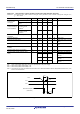
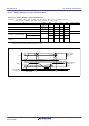
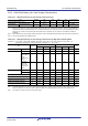
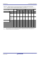
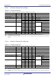
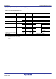
Table Of Contents
- 45. 12-Bit D/A Converter (R12DAA)
- 46. Temperature Sensor (TEMPSA)
- 47. Comparator B (CMPBa)
- 47.1 Overview
- 47.2 Register Descriptions
- 47.2.1 Comparator B1 Control Register 1 (CPB1CNT1)
- 47.2.2 Comparator B1 Control Register 2 (CPB1CNT2)
- 47.2.3 Comparator B1 Flag Register (CPB1FLG)
- 47.2.4 Comparator B1 Interrupt Control Register (CPB1INT)
- 47.2.5 Comparator B1 Filter Select Register (CPB1F)
- 47.2.6 Comparator B1 Mode Select Register (CPB1MD)
- 47.2.7 Comparator B1 Reference Input Voltage Select Register (CPB1REF)
- 47.2.8 Comparator B1 Output Control Register (CPB1OCR)
- 47.3 Operation
- 47.4 Comparator B2 and Comparator B3 Interrupts
- 47.5 Usage Note
- 48. Data Operation Circuit (DOC)
- 49. RAM
- 50. Flash Memory (FLASH)
- 50.1 Overview
- 50.2 ROM Area and Block Configuration
- 50.3 E2 DataFlash Area and Block Configuration
- 50.4 Register Descriptions
- 50.4.1 E2 DataFlash Control Register (DFLCTL)
- 50.4.2 Flash P/E Mode Entry Register (FENTRYR)
- 50.4.3 Protection Unlock Register (FPR)
- 50.4.4 Protection Unlock Status Register (FPSR)
- 50.4.5 Flash P/E Mode Control Register (FPMCR)
- 50.4.6 Flash Initial Setting Register (FISR)
- 50.4.7 Flash Reset Register (FRESETR)
- 50.4.8 Flash Area Select Register (FASR)
- 50.4.9 Flash Control Register (FCR)
- 50.4.10 Flash Extra Area Control Register (FEXCR)
- 50.4.11 Flash Processing Start Address Register H (FSARH)
- 50.4.12 Flash Processing Start Address Register L (FSARL)
- 50.4.13 Flash Processing End Address Register H (FEARH)
- 50.4.14 Flash Processing End Address Register L (FEARL)
- 50.4.15 Flash Write Buffer Register n (FWBn) (n = 0 to 3)
- 50.4.16 Flash Status Register 0 (FSTATR0)
- 50.4.17 Flash Status Register 1 (FSTATR1)
- 50.4.18 Flash Error Address Monitor Register H (FEAMH)
- 50.4.19 Flash Error Address Monitor Register L (FEAML)
- 50.4.20 Flash Start-Up Setting Monitor Register (FSCMR)
- 50.4.21 Flash Access Window Start Address Monitor Register (FAWSMR)
- 50.4.22 Flash Access Window End Address Monitor Register (FAWEMR)
- 50.4.23 Unique ID Register n (UIDRn) (n = 0 to 3)
- 50.5 Start-Up Program Protection
- 50.6 Area Protection
- 50.7 Programming and Erasure
- 50.8 Boot Mode
- 50.9 Flash Memory Protection
- 50.10 Communication Protocol
- 50.10.1 State Transition in Boot Mode (SCI Interface)
- 50.10.2 Command and Response Configuration
- 50.10.3 Response to Undefined Commands
- 50.10.4 Boot Mode Status Inquiry
- 50.10.5 Inquiry Commands
- 50.10.6 Setting Commands
- 50.10.7 ID Code Authentication Command
- 50.10.8 Program/Erase Commands
- 50.10.9 Read-Check Commands
- 50.11 Serial Programmer Operation in Boot Mode (SCI Interface)
- 50.11.1 Bit Rate Automatic Adjustment Procedure
- 50.11.2 Procedure to Receive the MCU Information
- 50.11.3 Procedure to Select the Device and Change the Bit Rate
- 50.11.4 Procedure for Transition to the Program/Erase Host Command Wait State
- 50.11.5 Procedure to Unlock Boot Mode ID Code Protection
- 50.11.6 Procedure to Erase the User Area and Data Area
- 50.11.7 Procedure to Program the User Area and Data Area
- 50.11.8 Procedure to Check Data in the User Area
- 50.11.9 Procedure to Check Data in the Data Area
- 50.11.10 Procedure to Set the Access Window in the User Area
- 50.12 Rewriting by Self-Programming
- 50.13 Usage Notes
- 50.14 Usage Notes in Boot Mode
- 51. Electrical Characteristics
- 51.1 Absolute Maximum Ratings
- 51.2 DC Characteristics
- 51.3 AC Characteristics
- 51.3.1 Clock Timing
- 51.3.2 Reset Timing
- 51.3.3 Timing of Recovery from Low Power Consumption Modes
- 51.3.4 Control Signal Timing
- 51.3.5 Timing of On-Chip Peripheral Modules
- 51.3.5.1 Timing of I/O Ports
- 51.3.5.2 Timing of MTU/TPU
- 51.3.5.3 Timing of POE
- 51.3.5.4 Timing of TMR
- 51.3.5.5 Timing of SCI
- 51.3.5.6 Timing of RIIC
- 51.3.5.7 Timing of RSPI
- 51.3.5.8 Timing of SSI
- 51.3.5.9 Timing of SDHI
- 51.3.5.10 Timing of A/D Converter Trigger
- 51.3.5.11 Timing of CAC
- 51.3.5.12 Timing of CLKOUT
- 51.3.5.13 Timing of CLKOUT_RF
- 51.4 USB Characteristics
- 51.5 A/D Conversion Characteristics
- 51.6 D/A Conversion Characteristics
- 51.7 Temperature Sensor Characteristics
- 51.8 Comparator Characteristics
- 51.9 CTSU Characteristics
- 51.10 Characteristics of Power-On Reset Circuit and Voltage Detection Circuit
- 51.11 Oscillation Stop Detection Timing
- 51.12 Battery Backup Function Characteristics
- 51.13 ROM (Flash Memory for Code Storage) Characteristics
- 51.14 E2 DataFlash Characteristics (Flash Memory for Data Storage)
- 51.15 BLE Characteristics
- 51.16 Usage Notes
- Appendix 1. Port States in Each Processing Mode
- Appendix 2. Package Dimensions
- REVISION HISTORY
- Colophon
- Address List
- Back cover

R01UH0823EJ0110 Rev.1.10 Page 1837 of 1852
Nov 30, 2020
RX23W Group 51. Electrical Characteristics
51.15 BLE Characteristics
51.15.1 Transmission Characteristics
Note: The characteristics are based on pins and functions other than those for the BLE interface not being in use.
Note 1. This does not take frequency errors due to manufacturing irregularities, drift with temperature, or deterioration of the crystal over
time into account.
51.15.2 Reception Characteristics (2 Mbps)
Note: The characteristics are based on pins and functions other than those for the BLE interface not being in use.
Note 1. PER ≤ 30.8%, and a 37-byte payload
Note 2. Allowable range of difference between the center frequency for the RF input signals and the carrier frequency generated within
the chip
Table 51.69 Transmission Characteristics
Conditions: VCC = VCC_RF = AVCC_RF = 3.3 V, VSS = VSS_RF = 0 V, T
a
= +25°C
Item Symbol Min. Typ. Max. Unit Test Conditions
Range of frequency RF
CF
2402 — 2480 MHz
Data rate RF
DATA_2M
— 2 — Mbps
RF
DATA_1M
— 1 — Mbps
RF
DATA_500k
— 500 — kbps
RF
DATA_125k
— 125 — kbps
Maximum transmitted output power RF
POWER
— 0 2 dBm 0 dBm output mode
— 4 6 dBm 4 dBm output mode
Output frequency error 85-pin BGA, 56-pin QFN RF
TXFERR
–10 — 10 ppm *
1
83-pin LGA RF
MTXFERR
–50 — 50 ppm T
a
: –40 to +85°C
Table 51.70 Reception Characteristics
Conditions: VCC = VCC_RF = AVCC_RF = 3.3 V, VSS = VSS_RF = 0 V, T
a
= +25°C
Item Symbol Min. Typ. Max. Unit Test Conditions
Input frequency RF
RXFIN_2M
2402 — 2480 MHz
Maximum input level RF
LEVL_2M
–10 4 — dBm *
1
Receiver sensitivity RF
STY_2M
— –92 — dBm *
1
Secondary emission strength RF
RXSP_2M
— –72 –57 dBm 30 MHz to 1 GHz
— –54 –47 dBm 1 GHz to 12 GHz
Co-channel rejection ratio RF
CCR_2M
— –8 — dB Prf = –67 dBm*
1
Adjacent channel rejection
ratio
RF
ADCR_2M
— 2 — dB Prf = –67 dBm*
1
±2 MHz
—35—dB ±4 MHz
—39—dB ±6 MHz
Blocking RF
BLK_2M
— –1 — dBm Prf = –67 dBm*
1
30 MHz to 2000 MHz
— –25 — dBm 2000 MHz to 2399 MHz
— –21 — dBm 2484 MHz to 3000 MHz
— –10 — dBm > 3000 MHz
Allowable frequency
deviation*
2
RF
RXFER_2M
–120 — 120 ppm *
1
RSSI accuracy RF
RSSIS_2M
— ±4 — dB –70 dBm ≤ Prf ≤ –10 dBm