
Users Manual
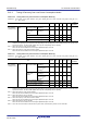
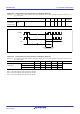
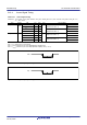
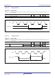
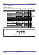
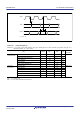
Table Of Contents
- 45. 12-Bit D/A Converter (R12DAA)
- 46. Temperature Sensor (TEMPSA)
- 47. Comparator B (CMPBa)
- 47.1 Overview
- 47.2 Register Descriptions
- 47.2.1 Comparator B1 Control Register 1 (CPB1CNT1)
- 47.2.2 Comparator B1 Control Register 2 (CPB1CNT2)
- 47.2.3 Comparator B1 Flag Register (CPB1FLG)
- 47.2.4 Comparator B1 Interrupt Control Register (CPB1INT)
- 47.2.5 Comparator B1 Filter Select Register (CPB1F)
- 47.2.6 Comparator B1 Mode Select Register (CPB1MD)
- 47.2.7 Comparator B1 Reference Input Voltage Select Register (CPB1REF)
- 47.2.8 Comparator B1 Output Control Register (CPB1OCR)
- 47.3 Operation
- 47.4 Comparator B2 and Comparator B3 Interrupts
- 47.5 Usage Note
- 48. Data Operation Circuit (DOC)
- 49. RAM
- 50. Flash Memory (FLASH)
- 50.1 Overview
- 50.2 ROM Area and Block Configuration
- 50.3 E2 DataFlash Area and Block Configuration
- 50.4 Register Descriptions
- 50.4.1 E2 DataFlash Control Register (DFLCTL)
- 50.4.2 Flash P/E Mode Entry Register (FENTRYR)
- 50.4.3 Protection Unlock Register (FPR)
- 50.4.4 Protection Unlock Status Register (FPSR)
- 50.4.5 Flash P/E Mode Control Register (FPMCR)
- 50.4.6 Flash Initial Setting Register (FISR)
- 50.4.7 Flash Reset Register (FRESETR)
- 50.4.8 Flash Area Select Register (FASR)
- 50.4.9 Flash Control Register (FCR)
- 50.4.10 Flash Extra Area Control Register (FEXCR)
- 50.4.11 Flash Processing Start Address Register H (FSARH)
- 50.4.12 Flash Processing Start Address Register L (FSARL)
- 50.4.13 Flash Processing End Address Register H (FEARH)
- 50.4.14 Flash Processing End Address Register L (FEARL)
- 50.4.15 Flash Write Buffer Register n (FWBn) (n = 0 to 3)
- 50.4.16 Flash Status Register 0 (FSTATR0)
- 50.4.17 Flash Status Register 1 (FSTATR1)
- 50.4.18 Flash Error Address Monitor Register H (FEAMH)
- 50.4.19 Flash Error Address Monitor Register L (FEAML)
- 50.4.20 Flash Start-Up Setting Monitor Register (FSCMR)
- 50.4.21 Flash Access Window Start Address Monitor Register (FAWSMR)
- 50.4.22 Flash Access Window End Address Monitor Register (FAWEMR)
- 50.4.23 Unique ID Register n (UIDRn) (n = 0 to 3)
- 50.5 Start-Up Program Protection
- 50.6 Area Protection
- 50.7 Programming and Erasure
- 50.8 Boot Mode
- 50.9 Flash Memory Protection
- 50.10 Communication Protocol
- 50.10.1 State Transition in Boot Mode (SCI Interface)
- 50.10.2 Command and Response Configuration
- 50.10.3 Response to Undefined Commands
- 50.10.4 Boot Mode Status Inquiry
- 50.10.5 Inquiry Commands
- 50.10.6 Setting Commands
- 50.10.7 ID Code Authentication Command
- 50.10.8 Program/Erase Commands
- 50.10.9 Read-Check Commands
- 50.11 Serial Programmer Operation in Boot Mode (SCI Interface)
- 50.11.1 Bit Rate Automatic Adjustment Procedure
- 50.11.2 Procedure to Receive the MCU Information
- 50.11.3 Procedure to Select the Device and Change the Bit Rate
- 50.11.4 Procedure for Transition to the Program/Erase Host Command Wait State
- 50.11.5 Procedure to Unlock Boot Mode ID Code Protection
- 50.11.6 Procedure to Erase the User Area and Data Area
- 50.11.7 Procedure to Program the User Area and Data Area
- 50.11.8 Procedure to Check Data in the User Area
- 50.11.9 Procedure to Check Data in the Data Area
- 50.11.10 Procedure to Set the Access Window in the User Area
- 50.12 Rewriting by Self-Programming
- 50.13 Usage Notes
- 50.14 Usage Notes in Boot Mode
- 51. Electrical Characteristics
- 51.1 Absolute Maximum Ratings
- 51.2 DC Characteristics
- 51.3 AC Characteristics
- 51.3.1 Clock Timing
- 51.3.2 Reset Timing
- 51.3.3 Timing of Recovery from Low Power Consumption Modes
- 51.3.4 Control Signal Timing
- 51.3.5 Timing of On-Chip Peripheral Modules
- 51.3.5.1 Timing of I/O Ports
- 51.3.5.2 Timing of MTU/TPU
- 51.3.5.3 Timing of POE
- 51.3.5.4 Timing of TMR
- 51.3.5.5 Timing of SCI
- 51.3.5.6 Timing of RIIC
- 51.3.5.7 Timing of RSPI
- 51.3.5.8 Timing of SSI
- 51.3.5.9 Timing of SDHI
- 51.3.5.10 Timing of A/D Converter Trigger
- 51.3.5.11 Timing of CAC
- 51.3.5.12 Timing of CLKOUT
- 51.3.5.13 Timing of CLKOUT_RF
- 51.4 USB Characteristics
- 51.5 A/D Conversion Characteristics
- 51.6 D/A Conversion Characteristics
- 51.7 Temperature Sensor Characteristics
- 51.8 Comparator Characteristics
- 51.9 CTSU Characteristics
- 51.10 Characteristics of Power-On Reset Circuit and Voltage Detection Circuit
- 51.11 Oscillation Stop Detection Timing
- 51.12 Battery Backup Function Characteristics
- 51.13 ROM (Flash Memory for Code Storage) Characteristics
- 51.14 E2 DataFlash Characteristics (Flash Memory for Data Storage)
- 51.15 BLE Characteristics
- 51.16 Usage Notes
- Appendix 1. Port States in Each Processing Mode
- Appendix 2. Package Dimensions
- REVISION HISTORY
- Colophon
- Address List
- Back cover

R01UH0823EJ0110 Rev.1.10 Page 1791 of 1852
Nov 30, 2020
RX23W Group 51. Electrical Characteristics
51.3.3 Timing of Recovery from Low Power Consumption Modes
Note 1. The recovery time varies depending on the state of each oscillator when the WAIT instruction is executed. When multiple
oscillators are operating, the recovery time varies depending on the operating state of the oscillators that are not selected as the
system clock source. The above table applies when only the corresponding clock is operating.
Note 2. When the frequency of the crystal is 20 MHz.
When the main clock oscillator wait control register (MOSCWTCR) is set to 04h.
Note 3. When the frequency of the external clock is 20 MHz.
When the main clock oscillator wait control register (MOSCWTCR) is set to 00h.
Note 1. The recovery time varies depending on the state of each oscillator when the WAIT instruction is executed. When multiple
oscillators are operating, the recovery time varies depending on the operating state of the oscillators that are not selected as the
system clock source. The above table applies when only the corresponding clock is operating.
Note 2. When the frequency of the crystal is 12 MHz.
When the main clock oscillator wait control register (MOSCWTCR) is set to 04h.
Note 3. When the frequency of PLL is 12 MHz.
When the main clock oscillator wait control register (MOSCWTCR) is set to 04h.
Note 4. When the frequency of the external clock is 12 MHz.
When the main clock oscillator wait control register (MOSCWTCR) is set to 00h.
Note 5. When the frequency of PLL is 12 MHz.
When the main clock oscillator wait control register (MOSCWTCR) is set to 00h.
Note 6. This is the case when HOCO is selected as the system clock and its frequency division is set to be 8 MHz.
Table 51.26 Timing of Recovery from Low Power Consumption Modes (1)
Conditions: 1.8 V ≤ VCC = VCC_USB = AVCC0 = VCC_RF = AVCC_RF ≤ 3.6 V, VSS = AVSS0 = VSS_USB = VSS_RF = 0 V,
T
a
= –40 to +85°C
Item Symbol Min. Typ. Max. Unit
Test
Conditions
Recovery time
from software
standby mode*
1
High-speed
mode
Crystal connected to
main clock oscillator
Main clock oscillator
operating*
2
t
SBYMC
— 2 3 ms Figure 51.30
External clock input
to main clock
oscillator
Main clock oscillator
operating*
3
t
SBYEX
—3550µs
Sub-clock oscillator operating t
SBYSC
— 650 800 µs
HOCO clock oscillator operating t
SBYHO
—4055µs
LOCO clock oscillator operating t
SBYLO
—4055µs
Table 51.27 Timing of Recovery from Low Power Consumption Modes (2)
Conditions: 1.8 V ≤ VCC = VCC_USB = AVCC0 = VCC_RF = AVCC_RF ≤ 3.6 V, VSS = AVSS0 = VSS_USB = VSS_RF = 0 V,
T
a
= –40 to +85°C
Item Symbol Min. Typ. Max. Unit
Test
Conditions
Recovery time
from software
standby mode*
1
Middle-speed
mode
Crystal connected to
main clock oscillator
Main clock oscillator
operating*
2
t
SBYMC
— 2 3 ms Figure 51.30
Main clock oscillator
and PLL circuit
operating*
3
t
SBYPC
—2 3ms
External clock input
to main clock
oscillator
Main clock oscillator
operating*
4
t
SBYEX
—3 4µs
Main clock oscillator
and PLL circuit
operating*
5
t
SBYPE
—6585µs
Sub-clock oscillator operating t
SBYSC
— 600 750 µs
HOCO clock oscillator operating*
6
t
SBYHO
—4050µs
LOCO clock oscillator operating t
SBYLO
—5 7µs