
Users Manual
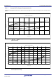
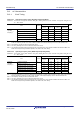
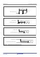
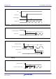
Table Of Contents
- 45. 12-Bit D/A Converter (R12DAA)
- 46. Temperature Sensor (TEMPSA)
- 47. Comparator B (CMPBa)
- 47.1 Overview
- 47.2 Register Descriptions
- 47.2.1 Comparator B1 Control Register 1 (CPB1CNT1)
- 47.2.2 Comparator B1 Control Register 2 (CPB1CNT2)
- 47.2.3 Comparator B1 Flag Register (CPB1FLG)
- 47.2.4 Comparator B1 Interrupt Control Register (CPB1INT)
- 47.2.5 Comparator B1 Filter Select Register (CPB1F)
- 47.2.6 Comparator B1 Mode Select Register (CPB1MD)
- 47.2.7 Comparator B1 Reference Input Voltage Select Register (CPB1REF)
- 47.2.8 Comparator B1 Output Control Register (CPB1OCR)
- 47.3 Operation
- 47.4 Comparator B2 and Comparator B3 Interrupts
- 47.5 Usage Note
- 48. Data Operation Circuit (DOC)
- 49. RAM
- 50. Flash Memory (FLASH)
- 50.1 Overview
- 50.2 ROM Area and Block Configuration
- 50.3 E2 DataFlash Area and Block Configuration
- 50.4 Register Descriptions
- 50.4.1 E2 DataFlash Control Register (DFLCTL)
- 50.4.2 Flash P/E Mode Entry Register (FENTRYR)
- 50.4.3 Protection Unlock Register (FPR)
- 50.4.4 Protection Unlock Status Register (FPSR)
- 50.4.5 Flash P/E Mode Control Register (FPMCR)
- 50.4.6 Flash Initial Setting Register (FISR)
- 50.4.7 Flash Reset Register (FRESETR)
- 50.4.8 Flash Area Select Register (FASR)
- 50.4.9 Flash Control Register (FCR)
- 50.4.10 Flash Extra Area Control Register (FEXCR)
- 50.4.11 Flash Processing Start Address Register H (FSARH)
- 50.4.12 Flash Processing Start Address Register L (FSARL)
- 50.4.13 Flash Processing End Address Register H (FEARH)
- 50.4.14 Flash Processing End Address Register L (FEARL)
- 50.4.15 Flash Write Buffer Register n (FWBn) (n = 0 to 3)
- 50.4.16 Flash Status Register 0 (FSTATR0)
- 50.4.17 Flash Status Register 1 (FSTATR1)
- 50.4.18 Flash Error Address Monitor Register H (FEAMH)
- 50.4.19 Flash Error Address Monitor Register L (FEAML)
- 50.4.20 Flash Start-Up Setting Monitor Register (FSCMR)
- 50.4.21 Flash Access Window Start Address Monitor Register (FAWSMR)
- 50.4.22 Flash Access Window End Address Monitor Register (FAWEMR)
- 50.4.23 Unique ID Register n (UIDRn) (n = 0 to 3)
- 50.5 Start-Up Program Protection
- 50.6 Area Protection
- 50.7 Programming and Erasure
- 50.8 Boot Mode
- 50.9 Flash Memory Protection
- 50.10 Communication Protocol
- 50.10.1 State Transition in Boot Mode (SCI Interface)
- 50.10.2 Command and Response Configuration
- 50.10.3 Response to Undefined Commands
- 50.10.4 Boot Mode Status Inquiry
- 50.10.5 Inquiry Commands
- 50.10.6 Setting Commands
- 50.10.7 ID Code Authentication Command
- 50.10.8 Program/Erase Commands
- 50.10.9 Read-Check Commands
- 50.11 Serial Programmer Operation in Boot Mode (SCI Interface)
- 50.11.1 Bit Rate Automatic Adjustment Procedure
- 50.11.2 Procedure to Receive the MCU Information
- 50.11.3 Procedure to Select the Device and Change the Bit Rate
- 50.11.4 Procedure for Transition to the Program/Erase Host Command Wait State
- 50.11.5 Procedure to Unlock Boot Mode ID Code Protection
- 50.11.6 Procedure to Erase the User Area and Data Area
- 50.11.7 Procedure to Program the User Area and Data Area
- 50.11.8 Procedure to Check Data in the User Area
- 50.11.9 Procedure to Check Data in the Data Area
- 50.11.10 Procedure to Set the Access Window in the User Area
- 50.12 Rewriting by Self-Programming
- 50.13 Usage Notes
- 50.14 Usage Notes in Boot Mode
- 51. Electrical Characteristics
- 51.1 Absolute Maximum Ratings
- 51.2 DC Characteristics
- 51.3 AC Characteristics
- 51.3.1 Clock Timing
- 51.3.2 Reset Timing
- 51.3.3 Timing of Recovery from Low Power Consumption Modes
- 51.3.4 Control Signal Timing
- 51.3.5 Timing of On-Chip Peripheral Modules
- 51.3.5.1 Timing of I/O Ports
- 51.3.5.2 Timing of MTU/TPU
- 51.3.5.3 Timing of POE
- 51.3.5.4 Timing of TMR
- 51.3.5.5 Timing of SCI
- 51.3.5.6 Timing of RIIC
- 51.3.5.7 Timing of RSPI
- 51.3.5.8 Timing of SSI
- 51.3.5.9 Timing of SDHI
- 51.3.5.10 Timing of A/D Converter Trigger
- 51.3.5.11 Timing of CAC
- 51.3.5.12 Timing of CLKOUT
- 51.3.5.13 Timing of CLKOUT_RF
- 51.4 USB Characteristics
- 51.5 A/D Conversion Characteristics
- 51.6 D/A Conversion Characteristics
- 51.7 Temperature Sensor Characteristics
- 51.8 Comparator Characteristics
- 51.9 CTSU Characteristics
- 51.10 Characteristics of Power-On Reset Circuit and Voltage Detection Circuit
- 51.11 Oscillation Stop Detection Timing
- 51.12 Battery Backup Function Characteristics
- 51.13 ROM (Flash Memory for Code Storage) Characteristics
- 51.14 E2 DataFlash Characteristics (Flash Memory for Data Storage)
- 51.15 BLE Characteristics
- 51.16 Usage Notes
- Appendix 1. Port States in Each Processing Mode
- Appendix 2. Package Dimensions
- REVISION HISTORY
- Colophon
- Address List
- Back cover

R01UH0823EJ0110 Rev.1.10 Page 1786 of 1852
Nov 30, 2020
RX23W Group 51. Electrical Characteristics
Note 1. Time until the clock can be used after the main clock oscillator stop bit (MOSCCR.MOSTP) is set to 0 (operating).
Note 2. Reference values when an 8-MHz resonator is used.
When specifying the main clock oscillator stabilization time, set the MOSCWTCR register with a stabilization time value that is
equal to or greater than the resonator-manufacturer-recommended value.
After the MOSCCR.MOSTP bit is changed to enable the main clock oscillator, confirm that the OSCOVFSR.MOOVF flag has
become 1, and then start using the main clock.
Note 3. The VCC range should be 2.4 to 3.6 V when the PLL is used.
Note 4. Reference values when a 32.768-kHz resonator is used.
After the setting of the SOSCCR.SOSTP bit or RCR3.RTCEN bit is changed to operate the sub-clock oscillator, only start using
the sub-clock after the sub-clock oscillation stabilization wait time that is equal to or greater than the oscillator-manufacturer-
recommended value has elapsed.
Note 5. The VCC range should be 3.0 to 3.6 V when the USBPLL is used.
Note 6. The oscillation frequency can be set to 48 MHz only.
Note 7. Only 32.768 kHz can be used.
Table 51.24 Clock Timing
Conditions: 1.8 V ≤ VCC = VCC_USB = AVCC0 = VCC_RF = AVCC_RF ≤ 3.6 V, VSS = AVSS0= VSS_USB = VSS_RF = 0 V,
T
a
= –40 to +85°C
Item Symbol Min. Typ. Max. Unit Test Conditions
EXTAL external clock input cycle time t
Xcyc
50 — — ns Figure 51.19
EXTAL external clock input high pulse width t
XH
20 — — ns
EXTAL external clock input low pulse width t
XL
20 — — ns
EXTAL external clock rise time t
Xr
—— 5 ns
EXTAL external clock fall time t
Xf
—— 5 ns
EXTAL external clock input wait time
*
1
t
XWT
0.5 — — µs
Main clock oscillator oscillation
frequency
*
2
2.4 ≤ VCC ≤ 3.6 f
MAIN
1—20MHz
1.8 ≤ VCC < 2.4 1 — 8
Main clock oscillation stabilization time (crystal)
*
2
t
MAINOSC
— 3 — ms Figure 51.20
Main clock oscillation stabilization time (ceramic
resonator)
*
2
t
MAINOSC
—50—µs
LOCO clock oscillation frequency f
LOCO
3.44 4.0 4.56 MHz
LOCO clock oscillation stabilization time t
LOCO
— — 0.5 µs Figure 51.21
IWDT-dedicated clock oscillation frequency f
ILOCO
12.75 15 17.25 kHz
IWDT-dedicated clock oscillation stabilization time t
ILOCO
— — 50 µs Figure 51.22
Bluetooth-dedicated clock oscillation frequency f
BLECK
—32—MHz
Bluetooth-dedicated low-speed on-chip oscillator
oscillation frequency
f
BLELOCO
— 32.768 — kHz
HOCO clock oscillation frequency f
HOCO
(32 MHz)
31.36 32 32.64 MHz T
a
= 0 to +85°C
31.04 32 32.96 T
a
= –40 to +85°C
f
HOCO
(54 MHz)
52.96 54 55.08 MHz T
a
= 0 to +85°C
52.38 54 55.62 T
a
= –40 to +85°C
HOCO clock oscillation stabilization time t
HOCO
— — 30 µs Figure 51.24
PLL input frequency
*
3
f
PLLIN
4 — 12.5 MHz
PLL circuit oscillation frequency
*
3
f
PLL
24 — 54 MHz
PLL clock oscillation stabilization time t
PLL
— — 50 µs Figure 51.25
PLL free-running oscillation frequency f
PLLFR
—8—MHz
USBPLL input frequency
*
5
f
PLLIN
— 4, 6, 8, 12 — MHz
USBPLL circuit oscillation frequency
*
5
f
PLL
— 48*
6
—MHz
USBPLL clock oscillation stabilization time t
PLL
— — 50 µs Figure 51.25
Sub-clock oscillator oscillation frequency
*
7
f
SUB
— 32.768 — kHz
Sub-clock oscillation stabilization time
*
4
t
SUBOSC
— 0.5 — s Figure 51.26