
Users Manual
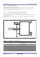
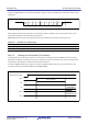
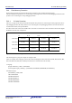
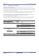
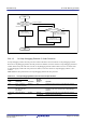
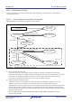
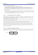
Table Of Contents
- 45. 12-Bit D/A Converter (R12DAA)
- 46. Temperature Sensor (TEMPSA)
- 47. Comparator B (CMPBa)
- 47.1 Overview
- 47.2 Register Descriptions
- 47.2.1 Comparator B1 Control Register 1 (CPB1CNT1)
- 47.2.2 Comparator B1 Control Register 2 (CPB1CNT2)
- 47.2.3 Comparator B1 Flag Register (CPB1FLG)
- 47.2.4 Comparator B1 Interrupt Control Register (CPB1INT)
- 47.2.5 Comparator B1 Filter Select Register (CPB1F)
- 47.2.6 Comparator B1 Mode Select Register (CPB1MD)
- 47.2.7 Comparator B1 Reference Input Voltage Select Register (CPB1REF)
- 47.2.8 Comparator B1 Output Control Register (CPB1OCR)
- 47.3 Operation
- 47.4 Comparator B2 and Comparator B3 Interrupts
- 47.5 Usage Note
- 48. Data Operation Circuit (DOC)
- 49. RAM
- 50. Flash Memory (FLASH)
- 50.1 Overview
- 50.2 ROM Area and Block Configuration
- 50.3 E2 DataFlash Area and Block Configuration
- 50.4 Register Descriptions
- 50.4.1 E2 DataFlash Control Register (DFLCTL)
- 50.4.2 Flash P/E Mode Entry Register (FENTRYR)
- 50.4.3 Protection Unlock Register (FPR)
- 50.4.4 Protection Unlock Status Register (FPSR)
- 50.4.5 Flash P/E Mode Control Register (FPMCR)
- 50.4.6 Flash Initial Setting Register (FISR)
- 50.4.7 Flash Reset Register (FRESETR)
- 50.4.8 Flash Area Select Register (FASR)
- 50.4.9 Flash Control Register (FCR)
- 50.4.10 Flash Extra Area Control Register (FEXCR)
- 50.4.11 Flash Processing Start Address Register H (FSARH)
- 50.4.12 Flash Processing Start Address Register L (FSARL)
- 50.4.13 Flash Processing End Address Register H (FEARH)
- 50.4.14 Flash Processing End Address Register L (FEARL)
- 50.4.15 Flash Write Buffer Register n (FWBn) (n = 0 to 3)
- 50.4.16 Flash Status Register 0 (FSTATR0)
- 50.4.17 Flash Status Register 1 (FSTATR1)
- 50.4.18 Flash Error Address Monitor Register H (FEAMH)
- 50.4.19 Flash Error Address Monitor Register L (FEAML)
- 50.4.20 Flash Start-Up Setting Monitor Register (FSCMR)
- 50.4.21 Flash Access Window Start Address Monitor Register (FAWSMR)
- 50.4.22 Flash Access Window End Address Monitor Register (FAWEMR)
- 50.4.23 Unique ID Register n (UIDRn) (n = 0 to 3)
- 50.5 Start-Up Program Protection
- 50.6 Area Protection
- 50.7 Programming and Erasure
- 50.8 Boot Mode
- 50.9 Flash Memory Protection
- 50.10 Communication Protocol
- 50.10.1 State Transition in Boot Mode (SCI Interface)
- 50.10.2 Command and Response Configuration
- 50.10.3 Response to Undefined Commands
- 50.10.4 Boot Mode Status Inquiry
- 50.10.5 Inquiry Commands
- 50.10.6 Setting Commands
- 50.10.7 ID Code Authentication Command
- 50.10.8 Program/Erase Commands
- 50.10.9 Read-Check Commands
- 50.11 Serial Programmer Operation in Boot Mode (SCI Interface)
- 50.11.1 Bit Rate Automatic Adjustment Procedure
- 50.11.2 Procedure to Receive the MCU Information
- 50.11.3 Procedure to Select the Device and Change the Bit Rate
- 50.11.4 Procedure for Transition to the Program/Erase Host Command Wait State
- 50.11.5 Procedure to Unlock Boot Mode ID Code Protection
- 50.11.6 Procedure to Erase the User Area and Data Area
- 50.11.7 Procedure to Program the User Area and Data Area
- 50.11.8 Procedure to Check Data in the User Area
- 50.11.9 Procedure to Check Data in the Data Area
- 50.11.10 Procedure to Set the Access Window in the User Area
- 50.12 Rewriting by Self-Programming
- 50.13 Usage Notes
- 50.14 Usage Notes in Boot Mode
- 51. Electrical Characteristics
- 51.1 Absolute Maximum Ratings
- 51.2 DC Characteristics
- 51.3 AC Characteristics
- 51.3.1 Clock Timing
- 51.3.2 Reset Timing
- 51.3.3 Timing of Recovery from Low Power Consumption Modes
- 51.3.4 Control Signal Timing
- 51.3.5 Timing of On-Chip Peripheral Modules
- 51.3.5.1 Timing of I/O Ports
- 51.3.5.2 Timing of MTU/TPU
- 51.3.5.3 Timing of POE
- 51.3.5.4 Timing of TMR
- 51.3.5.5 Timing of SCI
- 51.3.5.6 Timing of RIIC
- 51.3.5.7 Timing of RSPI
- 51.3.5.8 Timing of SSI
- 51.3.5.9 Timing of SDHI
- 51.3.5.10 Timing of A/D Converter Trigger
- 51.3.5.11 Timing of CAC
- 51.3.5.12 Timing of CLKOUT
- 51.3.5.13 Timing of CLKOUT_RF
- 51.4 USB Characteristics
- 51.5 A/D Conversion Characteristics
- 51.6 D/A Conversion Characteristics
- 51.7 Temperature Sensor Characteristics
- 51.8 Comparator Characteristics
- 51.9 CTSU Characteristics
- 51.10 Characteristics of Power-On Reset Circuit and Voltage Detection Circuit
- 51.11 Oscillation Stop Detection Timing
- 51.12 Battery Backup Function Characteristics
- 51.13 ROM (Flash Memory for Code Storage) Characteristics
- 51.14 E2 DataFlash Characteristics (Flash Memory for Data Storage)
- 51.15 BLE Characteristics
- 51.16 Usage Notes
- Appendix 1. Port States in Each Processing Mode
- Appendix 2. Package Dimensions
- REVISION HISTORY
- Colophon
- Address List
- Back cover

R01UH0823EJ0110 Rev.1.10 Page 1723 of 1852
Nov 30, 2020
RX23W Group 50. Flash Memory (FLASH)
As shown in Figure 50.25, set the format to 8-bit data, 1 stop bit, no parity, and LSB first to communicate with the serial
programmer.
Figure 50.25 Communication Format
Initial communication with the programmer is performed at 9,600 or 19,200 bps. The communication bit rate can be
changed after the MCU is connected with the programmer.
Table 50.11 lists the maximum communication bit rates for communication in boot mode (SCI interface).
50.8.2.2 Starting Up in Boot Mode (SCI Interface)
To start the MCU in boot mode (SCI interface), a reset must be released by changing the RES# pin from low to high
while both of the MD pin and UB pin are low. After starting up in boot mode (SCI interface), wait at least 400 ms until
communication with the MCU is enabled in boot mode (SCI interface).
As shown in
Figure 50.26, keep the signal of each pin unchanged for 400 ms after the reset is released. Use resets
according to the range described in
section 51.3.2, Reset Timing.
Figure 50.26 Wait Time until Communication Becomes Possible in Boot Mode (SCI Interface)
Table 50.11 Conditions for Communication
Operating Voltage Maximum Communication Bit Rate
Lower than 3.0 V 500 kbps
3.0 V or higher 2 Mbps
Start
bit
D0 D1 D2 D3 D4 D5 D6 D7
Stop
bit
System power supply
RES#
MD
UB
RXD1
TXD1
Low or open
Low
High
High
Communication starts
400 ms or longer