
Users Manual
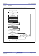
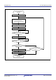
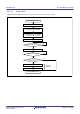
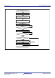
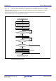
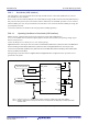
Table Of Contents
- 45. 12-Bit D/A Converter (R12DAA)
- 46. Temperature Sensor (TEMPSA)
- 47. Comparator B (CMPBa)
- 47.1 Overview
- 47.2 Register Descriptions
- 47.2.1 Comparator B1 Control Register 1 (CPB1CNT1)
- 47.2.2 Comparator B1 Control Register 2 (CPB1CNT2)
- 47.2.3 Comparator B1 Flag Register (CPB1FLG)
- 47.2.4 Comparator B1 Interrupt Control Register (CPB1INT)
- 47.2.5 Comparator B1 Filter Select Register (CPB1F)
- 47.2.6 Comparator B1 Mode Select Register (CPB1MD)
- 47.2.7 Comparator B1 Reference Input Voltage Select Register (CPB1REF)
- 47.2.8 Comparator B1 Output Control Register (CPB1OCR)
- 47.3 Operation
- 47.4 Comparator B2 and Comparator B3 Interrupts
- 47.5 Usage Note
- 48. Data Operation Circuit (DOC)
- 49. RAM
- 50. Flash Memory (FLASH)
- 50.1 Overview
- 50.2 ROM Area and Block Configuration
- 50.3 E2 DataFlash Area and Block Configuration
- 50.4 Register Descriptions
- 50.4.1 E2 DataFlash Control Register (DFLCTL)
- 50.4.2 Flash P/E Mode Entry Register (FENTRYR)
- 50.4.3 Protection Unlock Register (FPR)
- 50.4.4 Protection Unlock Status Register (FPSR)
- 50.4.5 Flash P/E Mode Control Register (FPMCR)
- 50.4.6 Flash Initial Setting Register (FISR)
- 50.4.7 Flash Reset Register (FRESETR)
- 50.4.8 Flash Area Select Register (FASR)
- 50.4.9 Flash Control Register (FCR)
- 50.4.10 Flash Extra Area Control Register (FEXCR)
- 50.4.11 Flash Processing Start Address Register H (FSARH)
- 50.4.12 Flash Processing Start Address Register L (FSARL)
- 50.4.13 Flash Processing End Address Register H (FEARH)
- 50.4.14 Flash Processing End Address Register L (FEARL)
- 50.4.15 Flash Write Buffer Register n (FWBn) (n = 0 to 3)
- 50.4.16 Flash Status Register 0 (FSTATR0)
- 50.4.17 Flash Status Register 1 (FSTATR1)
- 50.4.18 Flash Error Address Monitor Register H (FEAMH)
- 50.4.19 Flash Error Address Monitor Register L (FEAML)
- 50.4.20 Flash Start-Up Setting Monitor Register (FSCMR)
- 50.4.21 Flash Access Window Start Address Monitor Register (FAWSMR)
- 50.4.22 Flash Access Window End Address Monitor Register (FAWEMR)
- 50.4.23 Unique ID Register n (UIDRn) (n = 0 to 3)
- 50.5 Start-Up Program Protection
- 50.6 Area Protection
- 50.7 Programming and Erasure
- 50.8 Boot Mode
- 50.9 Flash Memory Protection
- 50.10 Communication Protocol
- 50.10.1 State Transition in Boot Mode (SCI Interface)
- 50.10.2 Command and Response Configuration
- 50.10.3 Response to Undefined Commands
- 50.10.4 Boot Mode Status Inquiry
- 50.10.5 Inquiry Commands
- 50.10.6 Setting Commands
- 50.10.7 ID Code Authentication Command
- 50.10.8 Program/Erase Commands
- 50.10.9 Read-Check Commands
- 50.11 Serial Programmer Operation in Boot Mode (SCI Interface)
- 50.11.1 Bit Rate Automatic Adjustment Procedure
- 50.11.2 Procedure to Receive the MCU Information
- 50.11.3 Procedure to Select the Device and Change the Bit Rate
- 50.11.4 Procedure for Transition to the Program/Erase Host Command Wait State
- 50.11.5 Procedure to Unlock Boot Mode ID Code Protection
- 50.11.6 Procedure to Erase the User Area and Data Area
- 50.11.7 Procedure to Program the User Area and Data Area
- 50.11.8 Procedure to Check Data in the User Area
- 50.11.9 Procedure to Check Data in the Data Area
- 50.11.10 Procedure to Set the Access Window in the User Area
- 50.12 Rewriting by Self-Programming
- 50.13 Usage Notes
- 50.14 Usage Notes in Boot Mode
- 51. Electrical Characteristics
- 51.1 Absolute Maximum Ratings
- 51.2 DC Characteristics
- 51.3 AC Characteristics
- 51.3.1 Clock Timing
- 51.3.2 Reset Timing
- 51.3.3 Timing of Recovery from Low Power Consumption Modes
- 51.3.4 Control Signal Timing
- 51.3.5 Timing of On-Chip Peripheral Modules
- 51.3.5.1 Timing of I/O Ports
- 51.3.5.2 Timing of MTU/TPU
- 51.3.5.3 Timing of POE
- 51.3.5.4 Timing of TMR
- 51.3.5.5 Timing of SCI
- 51.3.5.6 Timing of RIIC
- 51.3.5.7 Timing of RSPI
- 51.3.5.8 Timing of SSI
- 51.3.5.9 Timing of SDHI
- 51.3.5.10 Timing of A/D Converter Trigger
- 51.3.5.11 Timing of CAC
- 51.3.5.12 Timing of CLKOUT
- 51.3.5.13 Timing of CLKOUT_RF
- 51.4 USB Characteristics
- 51.5 A/D Conversion Characteristics
- 51.6 D/A Conversion Characteristics
- 51.7 Temperature Sensor Characteristics
- 51.8 Comparator Characteristics
- 51.9 CTSU Characteristics
- 51.10 Characteristics of Power-On Reset Circuit and Voltage Detection Circuit
- 51.11 Oscillation Stop Detection Timing
- 51.12 Battery Backup Function Characteristics
- 51.13 ROM (Flash Memory for Code Storage) Characteristics
- 51.14 E2 DataFlash Characteristics (Flash Memory for Data Storage)
- 51.15 BLE Characteristics
- 51.16 Usage Notes
- Appendix 1. Port States in Each Processing Mode
- Appendix 2. Package Dimensions
- REVISION HISTORY
- Colophon
- Address List
- Back cover

R01UH0823EJ0110 Rev.1.10 Page 1719 of 1852
Nov 30, 2020
RX23W Group 50. Flash Memory (FLASH)
50.8.1 Boot Mode (USB Interface)
The flash memory can be programmed and erased using the USB interface in boot mode (USB interface). The user
area and data area can be rewritten.
When a reset is released while the MD pin is low and the UB pin is high, the MCU starts in boot mode (USB interface).
Self-powered or bus-powered can be selected in accordance with the state of the UPSEL pin. When a reset is released
while the UPSEL pin is low, self-powered mode is selected. When a reset is released while the UPSEL pin is high, bus-
powered mode is selected.
Contact the manufacturer for details on the serial programmer (USB programmer).
50.8.1.1 Operating Conditions in Boot Mode (USB Interface)
USB0 is used for communication with the serial programmer in boot mode (USB interface).
4, 6, 8, 12, or 16 MHz can be used as the frequency input to the main clock oscillator. The operating voltage range is
between 3.0 V and 3.6 V.
Connect the UB pin to VCC directly or VCC via a resistor (pull up).
Figure 50.22 shows an Example of Pin Connections in Boot Mode (USB Interface) When Self-Powered. Table 50.8
lists Pin Handling in Boot Mode (USB Interface) When Self-Powered.
Figure 50.23 shows an Example of Pin
Connections in Boot Mode (USB Interface) When Bus-Powered.
Table 50.9 lists Pin Handling in Boot Mode (USB
Interface) in Bus-Powered Mode.
Examples of pin connections shown in
Figure 50.22 and Figure 50.23 are simplified circuits. Operations are not
guaranteed in all systems.
Figure 50.22 Example of Pin Connections in Boot Mode (USB Interface) When Self-Powered
MCU
VCC
USB0_VBUS
VCC_USB
UPSEL
RES#
UB
USB0_DP XTAL
USB0_DM
EXTAL
VCL
VSS_USB
MD
VSS
Reset circuit
(user logic)
Connection/disconnection
detection signal input
Data I/O
Data I/O
*1
*2
Note 1. Connect a 4, 6, 8, 12, or 16 MHz crystal, ceramic resonator or oscillator to the main clock oscillator.
Note 2. UPSEL is assigned to the same pin as NMI. This is an example when the falling edge is selected by the NMI
detection set bit.